Download
1 / 6
60 likes | 346 Views
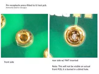
Pin receptacle press-fitted to IU test pcb . ( Partnumber detail on next page.). rear side w/ PMT inserted Note: This will not be visible on actual front PCB, it is buried in a blind hole. front side. Details of contact geometry. Cutaway view. (Necessary to solder body to a copper board

E N D
Pin receptacle press-fitted to IU test pcb. (Partnumber detail on next page.) rear side w/ PMT inserted Note: This will not be visible on actual front PCB, it is buried in a blind hole. front side
Details of contact geometry. Cutaway view. (Necessary to solder body to a copper board for fixturing for cutaway. Ignore this!) measured 0.090 inch
Contact with typical MCP-PMT pin inserted. ABSOLUTE MIN design insertion depth 0.100 inch first touch 0.068 inch (at this point of pin insertion, the contact beams are first observed to deflect)
Remarks: • Necessarily, the minimum design insertion depth is a judgement call. • If you ask the receptacle manufacturer, the answer will be larger still. • Someone has to make this judgement and be responsible for the consequences. • If you ask me, 0.100 inch (2.54 mm) is acceptable, based on my observations of the cutaway pin. A bit more would be better. • Lastly, please note that we are talking about the minimum design insertion depth, after all tolerances are taken into account.
From the above work, we set the position of PMT face with respect to the top surface of the front board 14.200 BASIC, as shown below.
And then the maximum allowable extent of the potting, measured from face of PMT, is simply defined by the need to not interfere with the pin receptacles or the front board. • A simple value of 13.489 mm maximum is acceptable (call it 13.45 mm for sanity). • Compare this to the HPK drawing, 13.80 mm. A change is necessary.