AMD Athlon XP Processor A Technical Brief
AMD Athlon XP Processor A Technical Brief. Badrinath Venkatesan Gurunath Rao Mallapragada. AMD Athlon XP Processor. Designed to meet the computation-intensive requirements of cutting-edge software application running on high-performance systems. Based on leading edge 0.13 micron technology

AMD Athlon XP Processor A Technical Brief
E N D
Presentation Transcript
AMD Athlon XP ProcessorA Technical Brief Badrinath Venkatesan Gurunath Rao Mallapragada CPE 631 HOMEWORK2 SPRING ‘04
AMD Athlon XP Processor • Designed to meet the computation-intensive requirements of cutting-edge software application running on high-performance systems. • Based on leading edge 0.13 micron technology • Increased on-chip cache • Maintains the stable and compatible Socket A infrastructure of AMD Athlon Processor. • Scalable and reliable for Business activities. • Delivers extremely high performance for Windows R XP. CPE 631 HOMEWORK2 SPRING ‘04
AMD Athlon XP • Manufactured on AMD’s advanced 0.13-micron copper process technology at AMD’s Fab 30 wafer fabrication facility in Dresden, Germany. • Die size: approximately 54.3 million transistors on 101 mm2 • It’s for desktop PC’s based on the “Barton” core. • Highly responsive system • World’s highest-performance PC processor CPE 631 HOMEWORK2 SPRING ‘04
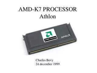
AMD Athlon XP 3200+512KB Cache / 400MHz FSB / Socket A / Barton Core / Processor CPE 631 HOMEWORK2 SPRING ‘04
Key Features • Advanced 400 Front-side System Bus to increase bandwidth. • 600 KB full-speed, on-chip cache to enable smooth and responsive 3-D gaming performance. • QuantiSpeedTM architecture. • 3DNow!TM Professional technology CPE 631 HOMEWORK2 SPRING ‘04
Increased FSB • Increase maximum data throughput into and out of the processor by up to 20 percentage over the 400MHz FSB. • Will gain significant performance on all types for software, including office productivity, digital media and 3-D gaming. • This processor outperforms its closest competitor by and average of 6 percent on a variety of industry-standard benchmarks. CPE 631 HOMEWORK2 SPRING ‘04
QuantiSpeedTM Architecture • Nine-issue superpipelined, superscalar x86 processor microarchitecture designed for high performance. • Multiple parallel x86 instruction decoders. • Three out-of order, superscalar, fully pipelined floating point execution units, which execute x87(floating point), MMX and 3DNow! • Three out-of-order, superscalar, pipelined integer units. CPE 631 HOMEWORK2 SPRING ‘04
QuantiSpeedTM Architecture • Three out-of-order, superscalar, pipelined address calculation units. • 7-entry instruction control unit. • Advance hardware data prefetch. • Exclusive and speculative Translation Look-aside Buffers. • Advance dynamic branch prediction. CPE 631 HOMEWORK2 SPRING ‘04
Real-World Application Performance The Application performance is a combination of two elements. • Clock frequency of the processor, measured in Megahertz or Gigahertz. • The amount of work the processor can accomplish in a given clock cycle, measured in instructions per clock cycle (IPC) CPE 631 HOMEWORK2 SPRING ‘04
Application Performance (cont..) • Clock frequency alone doesn’t determine application performance. • It’s the combination of both clock frequency and IPC. Application Performance = [clock frequency] X [work completed] Application Performance = GHz X IPC QuantiSpeed Architecture CPE 631 HOMEWORK2 SPRING ‘04
More on QuantiSpeed Architecture • QuantiSpeed architecture is the key element that provides AMD Athlon XP an edge out in the real world application for just two reason. • A balanced approach to optimize performance by increasing the amount of work done per clock cycle (IPC), while improving the operating frequency at the same time. CPE 631 HOMEWORK2 SPRING ‘04
Nine-issue, superscalar, Fully Pipelined Micro-architecture • Provides more pathway (pipelines) to feed instructions into the execution engine of the core. • Just allows the processor to complete more work in a given clock cycle (high IPC). • Balanced approach between pipeline depth and processor frequency to provide extraordinary levels of overall processor performance. CPE 631 HOMEWORK2 SPRING ‘04
Nine-issue, superscalar, Fully Pipelined Micro-architecture • Longer the pipelines => lower IPC and high operating frequency • Shorter the pipelines => increased IPC and lower operating frequency • This Nine-issue, superscalar, Fully Pipelined core is the heart of the QuantiSpeed architecture. CPE 631 HOMEWORK2 SPRING ‘04
Superscalar, Fully Pipelined Floating Point Unit (FPU) • More floating point operations per clock cycle than competitive x86 processor. • Permits high operating frequencies • The end result is the most powerful x86 FPU available today. • Provides computing power to tackle the most computation-intensive software applications. CPE 631 HOMEWORK2 SPRING ‘04
Hardware Data Prefetch • Gets data before the processor actually needs it. • Anticipates data the processor will need based on the executed instruction stream. • Prefetches data from main memory to the processor’s level 1 data cache (on-die cache memory) • Reduces the time it takes to feed the processor critical data, thus increasing throughput. CPE 631 HOMEWORK2 SPRING ‘04
Exclusive and Speculative TLBs • Keep the maps to critical data close to the processor. • Prevents the processor from stalling when future data is requested. • Large TLB’s give processors access to additional data maps. • Exclusive nature of TLB removes duplication of information CPE 631 HOMEWORK2 SPRING ‘04
Exclusive and Speculative TLBs • Exclusive nature frees up more space in L2 cache for other useful data to be used by the processor. • Speculation allows the processor to generate future maps of critical data quickly. • These features increases the work completed per clock cycle. • Improves real world application performance. CPE 631 HOMEWORK2 SPRING ‘04
Instruction Control Unit • Up to three mops per cycle are fetched to ICU. • It’s a 72-entry mops reorder buffer (ROB). ROB • Manages the execution of the mops. • Performs register renaming. • Controls exception (if any). • Manages instruction retirement operations. CPE 631 HOMEWORK2 SPRING ‘04
Execution Pipelines • 18 entry integer/address generation mop scheduler. • 36-entry floating point unit (FPU)/multimedia scheduler. • 9 independent execution pipelines. • Three for integer calculation. • Three for address calculation. • Three for execution of MMX, 3DNow! And x87 floating point instructions. CPE 631 HOMEWORK2 SPRING ‘04
Execution Pipelines • Three pipelined, out-of-order floating point execution units, each with a one-cycle throughput. • These three (FMUL, FADD, FSTORE) executes all x87 (floating point) instructions, MMX instructions, and enhanced 3DNow! Instructions. • The processor can deliver as many as four 32-bit, single-precision floating point result per clock cycle using a data format and SIMD. CPE 631 HOMEWORK2 SPRING ‘04
Sophisticated Dynamic branch predictors • To minimize or eliminate the delays due to branch instructions. • Includes • Branch Prediction table. • Branch target address table. • Return address stack. CPE 631 HOMEWORK2 SPRING ‘04
Sophisticated Dynamic branch predictors • Branch Prediction table • 2-way, 2048-entry. • Stores prediction information that is used for predicting the direction of conditional branches. • Branch target address table stores target addresses of conditional and unconditional branches. • Return address stack optimizes CALL/RET instruction pairs. • Stores the return address of each CALL. • Gives that to the corresponding RET instruction as predicted target address. CPE 631 HOMEWORK2 SPRING ‘04
3D Now! Technology • Significant innovation to x86 architecture which drives today’s PC’s. • Processor enhancement technology targeting the 3D-intensive calculations. • Group of new instructions that opens traditional bottlenecks for Multimedia and Floating Point intensive applications. • 3DNow! enables faster frame rates on high resolution screens, better modeling of real-world environments, sharper & detailed 3D imaging, smoother video playback and improved audio quality. CPE 631 HOMEWORK2 SPRING ‘04
3D Now! Technology Contd. • AMD played leading role in 3DNow! development. • Developed in coordination with OS designers. • Compatible with existing x86 software, requires no OS support. • Works with all existing OS. • AMD adds 5 new instructions to the existing 3DNow! Instruction set providing DSP extensions. CPE 631 HOMEWORK2 SPRING ‘04
3D Now! Key Functionality • Most advanced x86 processors have only one Floating Point execution unit. • A front end 3D Graphics software performs FP intensive operations. • FP operations are bottleneck in 3D graphics applications. Solution -- • Target FP operations to enhance performance. • Uses SIMD architecture to achieve enhanced performance. CPE 631 HOMEWORK2 SPRING ‘04
3D Now! Key Functionality • 26 SIMD instructions that support Floating Point operations. • With SIMD implementation each Floating Point instruction acts on two single-precision floating points. • Micro architecture can execute up to two 3DNow! Instructions per clock cycle through, two register pipelines. • Total four floating point operations per clock cycle!!! • 3DNow! Provides specific SIMD integer instruction to facilitate pixel-motion compensation, improving MPEG decoding. CPE 631 HOMEWORK2 SPRING ‘04
3DNow! Technology • MMX instructions were designed for integer intensive operations. • 3DNow! provides faster switch between x86 and MMX code with FEMMS(fast entry/exit multimedia state) instruction. • 3DNow! and MMX use same floating point registers so task switch between then is eliminated. • Facilitates faster voice recognition algorithms like IBM’s ViaVoice. • Reduces processor band width for decoding DVD tracks by 50%. CPE 631 HOMEWORK2 SPRING ‘04
3DNow! Technology • Media-based operations involve fetching large amounts of data from main memory. • The extra time involved in data fetch is reduced by using 3DNow! instruction call PREFETCH. • The existing MMX and 3DNow! instructions are merged, this means programs written in x86 can contain integer, MMX and floating point graphics instructions with no performance overhead. CPE 631 HOMEWORK2 SPRING ‘04
Enhanced 3DNow! Technology • Designed to take 3D multimedia performance to new heights. • Includes AMD’s original twenty-one 3DNow! Instructions. • Uses superscalar SIMD floating point techniques to accelerate 3D performance. • Twenty-four new instructions. CPE 631 HOMEWORK2 SPRING ‘04
Enhanced 3DNow! Technology - Functions • 52 SSE instructions with SIMD integer and floating point additions offer excellent compatibility with Intel’s SSE technology. • Provides powerful SIMD performance while enabling ease of implementation for software developers. • Compatible with Windows XP, ‘98, ’95 and NT 4.x operating system. CPE 631 HOMEWORK2 SPRING ‘04
Enhanced 3DNow Technology - Functions • 12 instructions that improve multimedia-enhanced integer math calculation used in speech reorganization and video processing. • 19 instructions that accelerate data movement for more detail graphics plug-ins • 5 DSP instructions to enhance the performance of communications applications. CPE 631 HOMEWORK2 SPRING ‘04
Data Format • 3DNow! Uses packed data format. • Data is packed in a single 64-bit 3DNow!/MMX register, comprising two IEEE 32-bit single precision double words. • Integers are packed as 8bitsX8, 64bitsX1 quad word, 32bitsX2 double words, 64bitsX1 quad word. CPE 631 HOMEWORK2 SPRING ‘04
System Bus Interface • 400 MHz, 333 MHz and 266 MHz system bus. • Enables excellent system bandwidth for data movement-intensive application. • Source synchronous clocking (clock forwarding) technology • Peak data rate of 3.2 GB/s • Support for 64-bit bi-directional data. CPE 631 HOMEWORK2 SPRING ‘04
System Bus Interface • The fastest bus implementation for x-86 platform. • Leverages the high-performance Digital Alpha EV6 system interface technology to boost the system performance. • Point-to-point topology for high data bandwidth independent of the number of processors. • Packet-based transfers for improved pipelining. CPE 631 HOMEWORK2 SPRING ‘04
System Bus Interface • Large burst data transfers. • 8-bit ECC protection of data and instructions. • Low-voltage signaling for high-performance. • Low-cost motherboard implementations. • Ability to address more than eight terabytes of physical memory. CPE 631 HOMEWORK2 SPRING ‘04
Socket A Infrastructure • Design are based on high-performance platforms and are supported by a full line of optimized infrastructure solutions (chipsets, motherboards, BIOS) • Available in Pin Grid Array (PGA) for mounting in a socketed infrastructure. • Electrical interface compatible with 333 MHz AMD XP system buses, based on Alpha EV6 bus protocol. CPE 631 HOMEWORK2 SPRING ‘04
Cache Architecture • Code named “Barton”, manufactured on state-of-the –art 130nm copper technology • Designed to meet the computationally intensive requirements of software applications • The AMD Athlon XP processor implements very large on-chip cache architecture for sustaining a highly superscalar microarchitecture • Particularly the L1 cache closest to the core CPE 631 HOMEWORK2 SPRING ‘04
Cache Architecture • The L1 cache is dual ported 128KB and split. • L1 cache has separate snoop ports • Snoop ports are designed to eliminate all coherency traffic from interfering with application performance • The L1 cache comprises of two 64KB data and instruction caches. • The instruction and data caches are two-way set-associative. • Much larger than Pentium4 L1( 128KB vs 8KB + 12KB micro ops). CPE 631 HOMEWORK2 SPRING ‘04
Cache Architecture • Due to large L1 cache, applications perform exceptionally fast as data and instructions are local to the processor. • The data cache has eight banks to provide maximum parallelism for running multiple applications. • The data cache supports concurrent access by two 64-bit loads or stores. • The instructions cache contains predecode data to assist multiple, high-performance instruction decoders. CPE 631 HOMEWORK2 SPRING ‘04
Cache Architecture • 512KB ,exclusive L2 cache. • L2 cache is 16-way set-associative . • Larger size helps increase performance of high-end gaming and digital media applications. • Higher associatively increases hit rate by reducing data conflicts. • As L2 is exclusive L1 data is not duplicated in L2, so we have total usable storage space of 640KB. • The AMD Athlon XP cache architecture also supports error correction code (ECC) protection. CPE 631 HOMEWORK2 SPRING ‘04
Processor Model CPE 631 HOMEWORK2 SPRING ‘04
Processor Model • Accelerated Graphics Port (AGP): This technology provides a dedicated, high-speed port for the movement of large blocks of 3D texture data between the PC's graphics controller and system memory. • AGP bus: is responsible for sending geometry data from system memory to the video card's frame buffer memory for processing by the graphics card's core. Theoretically, if more data can be transferred across this bus within a given time frame, it will allow for the graphics card to idle less and be fed a more steady stream of data. CPE 631 HOMEWORK2 SPRING ‘04
Processor Model • SCSI: SCSI is more of a system level interface, meaning that it does not only deal with disk drives. It is not a controller, like IDE, but a separate bus that is hooked to the system bus via a host adapter. A single SCSI bus can hold up to eight units, each with a different SCSI ID, ranging from 0 to 7. The host adapter takes up one ID, leaving 7 ID's for other hardware. Typical SCSI hardware includes hard drives, tape drives, CD-R/RW drives, scanners, etc. • EIDE – Enhanced IDE hard drive provides: • Increased maximum drive capacity • Faster data transfer • Secondary two-device channel • ATAPI (ATA Program Interface) CPE 631 HOMEWORK2 SPRING ‘04
Processor Model • BIOS: Basic Input-Output System. Part of the computer's operating system that is built into the machine, rather than read from a disk drive at startup • SDRAM or DDR:SDRAMs are based on standard dynamic RAM chips, but have sophisticated features that make them considerably faster. • First, SDRAM chips are fast enough to be synchronized with the CPU's clock, which eliminates wait states. • Second, the SDRAM chip is divided into two cell blocks, and data are interleaved between the two so that while a bit in one block is being accessed, the bit in the other is being prepared for access, allowing subsequent access to be faster CPE 631 HOMEWORK2 SPRING ‘04
Processor Model • LPC Bus: The Low Pin Count (LPC) bus interface was designed to enable a system without ISA or X-bus interfaces. The LPC interface will reduce the cost of traditional X-bus devices while meeting or exceeding the data transfer rate of X-bus. LPC will perform the same cycle types as the X-bus: Memory, I/O, DMA • USB: The Universal Serial Bus (USB) combines all of the advantages of a multiplatform standard—including decreased cost, increased compatibility, and a greater number of available peripherals • PCI Bus: Peripheral Component Interconnect Local Bus. A high speed avenue for transferring data between the CPU and peripherals. CPE 631 HOMEWORK2 SPRING ‘04
AMD Athlon XP Pipeline • The AMD Athlon processor contains two independent execution pipelines –one for integer operations and one for floating-point operations. • The integer pipeline manages all x86 integer operations. • The floating-point pipeline manages allx87, 3DNow! and MMX instructions. CPE 631 HOMEWORK2 SPRING ‘04
AMD Athlon XP Pipeline • The instruction fetch stage is one cycle long • The instruction alignment and decoding is four cycles long • The stage 5 (5th clock cycle) has three ports and provides maximum bandwidth of three MacroOPs per cycle for dispatching to the instruction control unit(ICU) CPE 631 HOMEWORK2 SPRING ‘04
AMD Athlon XP Pipeline Fetch/Scan/Align/Decode Hardware CPE 631 HOMEWORK2 SPRING ‘04
Fetch/Scan/Align/Decode Stages CPE 631 HOMEWORK2 SPRING ‘04
AMD Athlon XP Pipeline DirectPath & VectorPath • The most common x86 instructions flow through DirectPath pipeline stages and are decoded by hardware. • The less common instructions, requiring microcode assistance, flow through the VectorPath. • The DirectPath decodes common x86 instructions but also contains VectorPath instruction data, allowing it to maintain dispatch order at the end of cycle 5. CPE 631 HOMEWORK2 SPRING ‘04

