Download
1 / 10
100 likes | 160 Views
Wafer World provides wafers with the unique specification to meet customer needs. You can buy custom diameter wafers, thick wafers, thin wafers, double side polish wafers and other custom wafers online at the lowest prices. Call (561) 842-4441 today to know more.

E N D
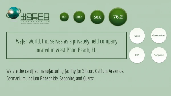
Wafer World, Inc. serves as a privately held company located in West Palm Beach, FL. We are the certified manufacturing facility for Silicon, Gallium Arsenide, Germanium, Indium Phosphide, Sapphire, and Quartz.
About silicon It is a chemical element that makes up almost 30% of the earth’s crust. Next to oxygen, it is the most abundant element in nature. Purpose of silicon wafers It is well known that most of the electronic devices are made up of semiconductors and microchips with despite the fact that on its own, it doesn’t conduct electricity very well. Before a semiconductor can be built though, the silicon must be turned into a wafer.
Silicon wafer manufacturing process 1. Ingot Growth 2. Slicing 3. Lapping 4. Cleaning 5. Polishing
Ingot Growth 1 Growing a silicon ingot can range in time from one week to one month depending on factors such as size, quality, and specification. More than 75% of silicon wafers grow via the Czochralski (CZ) method.
Slicing 2 After ingot growth process, the ingot is sliced by using a diamond edge saw.
Lapping 3 After the wafer has been sliced, it gets lapped. The lapping process removes saw marks and surface defects from the wafer. Wafer diameter
Cleaning 4 After lapping, the silicon wafers go through the process of being cleaned and etched. Sodium hydroxide or acetic and nitric acids alleviate any microscopic cracks and/or surface damage that may have come about during lapping.
Polishing 5 The final, and arguably most crucial step is the polishing of the silicon wafer. The polishing process takes place in a clean room where the workers wear cleanroom suits that cover their entire bodies.
Order Your Silicon Wafer Today (561) 842-4441 Call us at Visit our website www.waferworld.com Location 1100 Technology Place, Suite 104 West Palm Beach, FL 33407