Download
1 / 21
210 likes | 352 Views
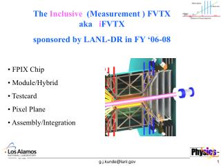
The Inclusive (Measurement ) FVTX aka i FVTX sponsored by LANL-DR in FY ‘06-08. FPIX Chip Module/Hybrid Testcard Pixel Plane Assembly/Integration. The Interaction Region at Phenix. Space for Vertex upgrade detectors. Outline. From Hybrid to Module From Module to Testcard

E N D
The Inclusive (Measurement ) FVTX aka iFVTX sponsored by LANL-DR in FY ‘06-08 • FPIX Chip • Module/Hybrid • Testcard • Pixel Plane • Assembly/Integration g.j.kunde@lanl.gov
The Interaction Region at Phenix Space for Vertex upgrade detectors g.j.kunde@lanl.gov
Outline • From Hybrid to Module • From Module to Testcard • From Testcard to Pixel Plane • From Pixel Plane to Station • From Station to Full Detector g.j.kunde@lanl.gov
Wire bonds Silicon Sensor FPIX2 HDI Support Structure Pixel Module VTT NOT TO SCALE g.j.kunde@lanl.gov
Dimensions: 111.0mm x 11.1mm + 2x 10.0mm x 11.1 mm tabs • Line width: 50m • Line to line clearance: 50m • Metal layer thickness: 12m • Number of layers: 4 • Via pad/hole: 150/70m • Lamination: 25m epoxy • Film thickness (polymide): 50m 8 Chip Module HDI designed by Fermilab/ made by (?) Mircoconex/Dyconex /CERN: HDI CAD top layer. HDI + 8 bare die chips. HDI + 8 chips with detector. (SINTEF PSPRAY) Several iterations, now minimal HDI g.j.kunde@lanl.gov
Production Flow • Chip and Sensor Test • Hybridization by VTT • Hybrid Test • HDI Electrical Test • Module Assembly • Test-card Assembly • Test and Burn-in • Pixel Plane Assembly • Test and Burn-in g.j.kunde@lanl.gov
Pixel Module Assembly • Fixture with Vaccum Chuck • Gluing of FPIX to HDI g.j.kunde@lanl.gov
Testcard and Wire Bonding • Testcard for each module • Gluing of module to card • Wirebonding of HDI to card g.j.kunde@lanl.gov
Ready Test Card g.j.kunde@lanl.gov
http://www-ese.fnal.gov/Phenix/PingaHelp/index.html PCI-based Test stands – PTA card • Perform module test • ‘PINGA’ test software • Initial characterization with inject pulser • Hit map • Absolute calibration • Burn-in (normal operation for 72 hours) • Repeat hit map • Q&A and module classification g.j.kunde@lanl.gov
Module Removal for Plane Assembly g.j.kunde@lanl.gov
4 Stations in FVTX Frame • 2 Planes per Station • 6 Identical Planes for Stations 2,3,4 • Smaller Plane for Station 1 • Room Temperature g.j.kunde@lanl.gov
PCB Power Bias Pulser TPG Cooling FPIX on HDI Voltage LVDS Output The Layout of a Plane g.j.kunde@lanl.gov
The Actual Plane and Stations • Flex Blades (Temperature compensation) • Two Planes Sandwich to get Station • Modules Inside • Connectors Outside g.j.kunde@lanl.gov
Large Pixel Plane (10 modules) Active components are Repeater and Regulator Delivery Imminent g.j.kunde@lanl.gov
Small Pixel Plane Concept (4-5 Modules) g.j.kunde@lanl.gov
PEEK tube Sensor Readout Chip TPG HDI Module Mounting and Cooling Placing and wirebonding Cooling with Fluor-carbon at temperature that keeps the HDI at assembly temperature g.j.kunde@lanl.gov
Cables to Pole Face • Five flat cables either side of active area on plane • 20 per large station, 12 per small station , total 72 • 48 low voltage, high voltage cables g.j.kunde@lanl.gov
Status and Plans • Status • All FPIXs are procured • All Si-detectors are procured • 15 Hybrids are delivered • 25 HDIs delivered, preparing production order • 10 module PCBs delivered • Several test cards are ready • Wire bonding at Si-det • Test stands are ready • Assembly gigs are ready g.j.kunde@lanl.gov
Preproduction and Production Plan • Production • TPG • TPG + Cooling • Test • PCB 3 small - 6 large • Mate PCB TPG • Test • 88 Modules on Cards • Test • Assemble Planes • Test • Assemble Stations • Cage • Assemble Detector • Proto (spare) • TPG • TPG + Cooling • Test • PCB • Mate PCB TPG • Test • 15 Modules on Cards • Test • Assemble Plane • Test • 15 FPIX only Modules on Cards • Test • Assemble Plane • Test VTT Rework ? g.j.kunde@lanl.gov
iFVTX 4 Pixel Planes 20 Module Station FPIX 2.1 8 chip module g.j.kunde@lanl.gov