Digital Logic Design 234262
300 likes | 502 Views
Digital Logic Design 234262. Alex Bronstein. Lecture 3: Memory and Buses. Abstraction Hierarchy. Application Software Operating System ( threads, files, exceptions ) Computer Architecture ( instruction set ) Micro-Architecture ( execution pipeline )

Digital Logic Design 234262
E N D
Presentation Transcript
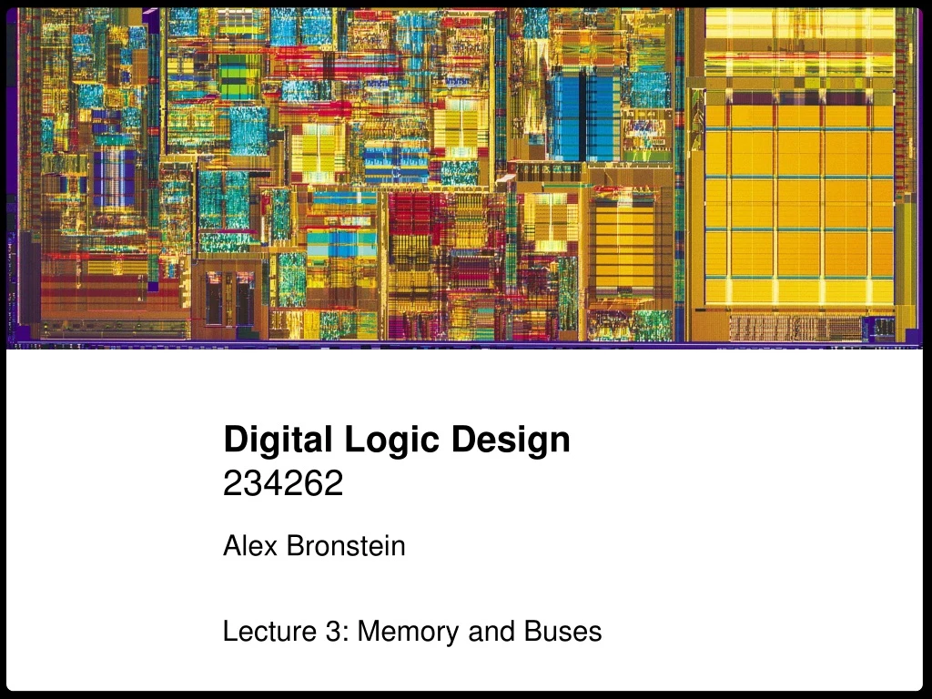
Digital Logic Design 234262 Alex Bronstein Lecture 3: Memory and Buses
Abstraction Hierarchy Application Software Operating System (threads, files, exceptions) Computer Architecture (instruction set) Micro-Architecture (execution pipeline) Logic (adders, multipliers, FSMs) Digital Circuits (gates) Analog Circuits (amplifiers) Process and Devices (MOS FET transistors) Physics (electrons, holes, tunneling, band gap)
Reminder: D Flip Flop • Positive edge-triggered D flip-flop (DFF) • Logical characteristic: • Output Q assumes the value of D after CLK rise • Timing characteristic: • If input is held constant tSUbefore • and tHafter clock rise then • old output will stay valid at least tcCQ • and new output will become valid • at most tpCQ after clock rise CLK CLK tSU tH D NEW tcCQ D Q Q OLD NEW tpCQ
Under the Hood • 1 DFF = 2×gated D-latches • Based on positive feedback • of inverting gates • ~20 transistors / bit of memory • Pros: • Fast! • Cons: • Chip area (=$) • Power
Memory Array • Many circuits can be shared in • a memory array • N address bits (2N addresses) • M bits word width • Decoder selects and asserts • a wordline • Data stored in bit cells are transferred • to or from bitlines • One word can be accessed at a time • Memories differ mainly by the bit cell structure 0 wordline 0 1 N stored bit cell ADDR . . . N:2N DECODER bitline 0 2N DM-1 D1 D0
Multi-Ported Memory Array N N A2 A1 N:2N DECODER N:2N DECODER D0 • Allows more than one word to be accessed at the same time • Used for register files and video memories
Illustrative Read Cycle N tRC WE3 A1 M N A1 RD1 A2 M tOH tAA N RD2 A3 N RD1 OLD DATA DATA VALID WD CLK • 2 read ports: Address A1 onto data output RD1, A2 onto RD2 • Read cycle is driven by address line • tRC– read cycle time • tAA – address access time (propagation delay) • tOH– output hold from address change (contamination delay)
Illustrative Write Cycle CLK N WE3 A1 M N RD1 A2 WE3 M tWR tAS N RD2 A3 M A3 WD tDW tDH CLK WD DATA VALID • 1 write port: Writes data WD onto address A3 on clock rising edge if write enable WE3 is asserted • tAS– address setup before WE3 is asserted • tWR– write recovery (address hold) • tDW, tDH – write data setup/hold times
Memory Types • Random Access Memory (RAM) – volatile • Static RAM (SRAM) • Dynamic RAM (DRAM) • Read-Only Memory (ROM) – non-volatile • ROM • Programmable ROM (PROM) • One-time programmable (OTP) • Erasable PROM (EPROM) • Electrically Erasable PROM (EEPROM) • Flash Memory
Static Memory (SRAM) • Cross-coupled inverters to store bit • 2 access transistors to read/write data • 6 transistors / bit • Multiported SRAM is used to implement • register files • Pros: • Fast (but slower than FF) • Cons: • Chip area (but less than FF) bitline bitline wordline
Dynamic Memory (DRAM) • Capacitor to store bit • Access transistor to read/write data • Read is destructive • Pros: • Area • Cost • Cons: • Slow (output not actively driven by a transistor) • Power (due to refresh) • More complicated controllers • Row open latencies bitline wordline
Non-Volatile Memory (ROM) • Access transistor: 0 bit • No transistor: 1 bit • Content established at manufacturing • Fuse programmable ROM • (aka one-time programmable, OTP): • Transistor is present in all cells • Fuse blown once to program content bitline bitline wordline bit 0 bit 1 bitline bitline wordline bit 0 bit 1
EPROM/EEPROM • Floating gate transistor • Programming by application of higher voltage • (hot charge injection into floating gate) • Erasure by • EPROM: exposing the die to UV light • EEPROM: applying reverse voltage (electron tunneling from • floating gate) bitline wordline
Look-up Table (LUT) • ROM can implement any CL function • N-bit address, M-bit word width = N-bit input, M-bit output • Often used for controllers, FSMs, nonlinear transformations • Depending on the function, logic/arithmetic implementation might be advantageous
System Bus • From Latin omnibus (=“for all”); English plural: buses or busses • A communication system connecting internal components of a computer • Common data highway is cheaper than many point-to-point links SECOND. MEMORY PRIMARY MEMORY CPU I/O CONTROL ADDRESS DATA
System Bus SECOND. MEMORY PRIMARY MEMORY CPU I/O CONTROL ADDRESS DATA • Address bus – selects device (and address within) • Control bus – specifies what action the device needs to perform • Data bus – transfers data
Master and Slave SECOND. MEMORY PRIMARY MEMORY CPU I/O READ WRITE CONTROL 123FA ADDRESS <DATA> DATA • Electrically a bus is a wire (actually, a bundle thereof) • Bus master – device that drives the bus (its output sets the voltage) • Bus slave – device that is driven by the bus (its input receives the signals from the bus)
Tri-State Logic 1 1 0 X 1 BUS 1 RAM OUTPUT CPU OUTPUT
Tri-State Logic EN EN • Add Enable signal to disconnect output from the bus • When disconnected, the output is floating (high impedance, high Z)
Tri-State Logic Tri-state buffers Tri-state inverters Active high enable Active low enable Active high enable Active low enable X Y X Y X Y X Y _ _ E E E E _ _ E X Y 0 0 Z 0 1 Z 1 0 0 1 1 1 E X Y 0 0 0 0 1 1 1 0 Z 1 1 Z E X Y 0 0 Z 0 1 Z 1 0 1 1 1 0 E X Y 0 0 1 0 1 0 1 0 Z 1 1 Z • Tri-state logic can be in 3 states: 0, 1, and Z • Buffers amplify signal, improve fanout and isolate systems • Inverters further invert output
Bidirectional Tristate Buffer to bus direction bus from bus • Allows to access the bus for reading or writing
Bus Arbiter • A multi-master bus requires an arbiterto decide which master is going • to control the bus at each clock cycle • Arbiter can be centralized (a dedicated circuit) such as in PCI, or • decentralized implementing some handshake protocol
Direct Memory Access (DMA) • Using the CPU to directly control I/O devices can be very costly • It would be better if an I/O device (e.g., a harddrive) could transfer data directly to/from RAM without the CPU needing to execute any in/out instructions • Direct Memory Access Controller (DMAC) has the capability to become the bus master to control the bus to transfer data between I/O device and memory • CPU sets up the DMAC to transfer a sequence of bytes • DMAC can handle several concurrent transfers (channels) competing over the bus
DMAC Bus Arbitration I/O Device DMAC Memory CPU DMA Request Hold Request asserted Hold Acknowledge asserted DMA Acknowledge Data transfer via bus . . . Cycle stealing Data transfer via bus Hold Request deasserted Hold Acknowledge deasserted
