Download
1 / 1
10 likes | 192 Views
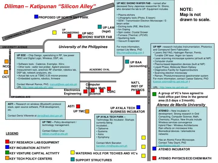
UP NEC SHONO WAFER FAB – named after deceased Sony Japanese researcher Dr. Shono, who donated the lab to UP. Equipment includes Plasma etchers Lithography tools (Photo, E-beam) SEM / Transmission Electron Microscope / E-beam writer Etching tools (RIE, Wet Etch) Ion Doping

E N D
UP NEC SHONO WAFER FAB – named after deceased Sony Japanese researcher Dr. Shono, who donated the lab to UP. Equipment includes • Plasma etchers • Lithography tools (Photo, E-beam) • SEM / Transmission Electron Microscope / E-beam writer • Etching tools (RIE, Wet Etch) • Ion Doping • Spin coater, Crystal Grower • Furnace (Thermal, LPCVD) • Sputtering tools • Vacuum Evaporator • For more information, • contact Lito Mena, PhD • (lito.mena@analog.com ) • UP NIP –research includes Instrumentation, Photonics and Compound Semi Fabrication. • Lasers (Nd:YAG, Hydrogen Raman, Femto, • Tunable CW laser, Argon ion lasers • Laser scanning microscope systems (all built at NIP) • Computer cluster • Plasma-based deposition devices (built at NIP) • Liquid Phase, Molecular Beam Epitaxy • Diagnostics Facility for Superconductors • Scanning electron microscopy • Raman, Photoluminescence spectrometer system • For more information, contact Caesar Saloma, PhD (caesar.saloma@nip.upd.edu.ph ) • URL : http://www.nip.upd.edu.ph • UP EEE – Chip Design, specializing in RF, low power RISC and Digital Logic, Wireless, DSP, etc. • Software tools : Cadence, Exemplar, Xilinx • Other tools : wafer test prober, Agilent precision measurement rack, anechoic RF chamber, robotics lab, DSP lab, network analyzers, etc. • Actual fab runs at TSMC 0.25 micron process • Embedded systems, robotics, firmware • Contact Manuel Ramos, PhD, manuel@eee.upd.edu.ph • URL http://www.upd.edu.ph/~eee/ ASTI – Research on wireless (Bluetooth) protocol stack, open source software, PCB development, etc. Contact Denis Villorente at denis@asti.dost.gov.ph • UP AYALA TECH PARK – Technology Biz incubator. Startups currently being • incubated… • Optiserve • Systema • Astra • Symphony • Contact Michi Barcelon • barcelon.mm@ayala.com.ph ATENEO – New incubator in development. Strong research in Grid Computing, Computer Science, Math, Chemistry, Physics. New thrusts include Wireless services convergence Hybrid Fiber / Wireless Architectures Rain effects on microwave links Biomedical devices / telemedicine networks Has an Atomic Force Microscope. Contact Toby Dayrit, PhD toby@admu.edu.ph UP TMC – Policy development / technology management. Contact Edison Cruz edison.cruz@up.edu.ph PROPOSED UP NORTH S&T PARK KEY INCUBATION ACTIVITY Diliman – Katipunan “Silicon Alley” NOTE: Map is not drawn to scale. K A T I P U N A N A V E COMMONWEALTH AVE UP LAW (legal) UP ENGINEERING UP NEC SHONO WAFER FAB University of the Philippines UNIVERSITY AVENUE UP BAA (accounting) NCC ACADEMIC OVAL CP GARCIA AVE CICT NAT’L INST OF PHYSICS Computer Science Math Electronics Engineering CSRC A group of VC’s have agreed to hold office part time in the general area (0.5 days x 2/month). Science CP GARCIA AVE Ateneo de Manila University ASTI UP AYALA TECHBUSINESS INCUBATOR UP TMC LEGEND KEY RESEARCH LAB/EQUIPMENT ATENEO INCUBATOR KEY VENTURE CAPITAL ACTIVITY WATERING HOLE FOR TECHIES AND VC’s ATENEO PHYSICS/ECE/CHEM/MATH KEY TECH POLICY CENTERS SUPPORT STRUCTURES