Memory and Caching
Memory and Caching. Chapter 7.1-7.6. The Memory Hierarchy. Registers L1 Cache L2 Cache Main memory Disk cache Disk Optical Tape. As one goes down the hierarchy Decreasing cost per bit Increasing capacity Increasing access time

Memory and Caching
E N D
Presentation Transcript
Memory and Caching Chapter 7.1-7.6
Registers L1 Cache L2 Cache Main memory Disk cache Disk Optical Tape As one goes down the hierarchy Decreasing cost per bit Increasing capacity Increasing access time Decreasing frequency of access of the memory by the processor – locality of reference Hierarchy List
So you want fast? • It is possible to build a computer which uses only static RAM (see later) • This would be very fast • This would need no cache • How can you cache cache? • This would cost a very large amount
Locality of Reference • Temporal Locality • Programs tend to reference the same memory locations at a future point in time • Due to loops and iteration, programs spending a lot of time in one section of code • Spatial Locality • Programs tend to reference memory locations that are near other recently-referenced memory locations • Due to the way contiguous memory is referenced, e.g. an array or the instructions that make up a program • Locality of reference does not always hold, but it usually holds
Cache Example • Consider a Level 1 cache capable of holding 1000 words with a 0.1 s access time. Level 2 is memory with a 1 s access time. • If 95% of memory access is in the cache: • T=(0.95)*(0.1 s) + (0.05)*(0.1+1 s) = 0.15 s • If 5% of memory access is in the cache: • T=(0.05)*(0.1 s) + (0.95)*(0.1+1 s) = 1.05 s • Want as many cache hits as possible! 1.1 s 0.1 s 100% 0%
Semiconductor Memory • RAM – Random Access Memory • Misnamed as all semiconductor memory is random access • Read/Write • Volatile • Temporary storage • Two main types: Static or Dynamic
Dynamic RAM • Bits stored as charge in semiconductor capacitors • Charges leak • Need refreshing even when powered • Simpler construction • Smaller per bit • Less expensive • Need refresh circuits (every few milliseconds) • Slower • Main memory
Static RAM • Bits stored as on/off switches via flip-flops • No charges to leak • No refreshing needed when powered • More complex construction • Larger per bit • More expensive • Does not need refresh circuits • Faster • Cache
Read Only Memory (ROM) • Permanent storage • Microprogramming • Library subroutines • Systems programs (BIOS) • Function tables
Types of ROM • Written during manufacture • Very expensive for small runs • Programmable (once) • PROM • Needs special equipment to program • Read “mostly” • Erasable Programmable (EPROM) • Erased by UV • Electrically Erasable (EEPROM) • Takes much longer to write than read • Flash memory • Erase whole memory electrically
Chip Organization • Consider an individual memory cell. Select line indicates if active, Control line indicates read or write. Control (WR) Cell Select (CS) Data In / Data Out (sense) Let’s say that each cell outputs 4 bits (i.e. word size=4 bits), and we would like to hook four of these together for a 4 word memory…
Four Word Memory, 4 bits per word Memory addresses: 0 A1=0, A0=0 1 A1=0, A0=1 2 A1=1, A0=0 3 A1=1, A0=1 Data from memory: Q3, Q2, Q1, Q0 Decoder selects only one memory cell
Simplified Representation • What one would see if this was packaged together
Constructing Wider Memory • Can pair two of our 4 word x 4 bit chips to make a 4 word x 8 bit chip : Use both in parallel
Constructing Longer Memory • We can combine chips to create a 8 word x 4 bit memory. Third address bit goes to a decoder to select only one of the two chips.
Splitting into Rows and Columns • Since most ICs are roughly square, many chips are constructed as a matrix of cells selectable by row and by column • RAS : Row Address Select • CAS : Column Address Select • 2 ½ - D organization
Refreshing • Refresh circuit included on chip • Disable chip • Count through rows • Read & Write back • Takes time • Slows down apparent performance
Packaging CE = Chip Enable, Vss = Ground, Vcc=+V, OE = Output Enable, WE = Write Enable
Module Organization • Combining RAS/CAS organization into Modules to reference 256K 8 bit words • 8 256K chip for each bit of the desired 8 bit word • Full 18 bit address presented to each module, a single bit output. Data distributed across all chips for a single word
Module Organization – Larger Memories • Can piece together existing modules to make even larger memories • Consider previous 256K x 8bit system • If we want 1M of memory, can tie together four of the 256K x 8bit modules • How to tell which of the four modules contains the data we want? • Need 20 address lines to reference 1M • Use lower 18 bits to reference address as before • Use higher 2 bits into the Chip Select to enable only one of the four memory modules
Cache • Small amount of fast memory • Sits between normal main memory and CPU • May be located on CPU chip or module
Cache operation - overview • CPU requests contents of memory location • Check cache for this data • If present, get from cache (fast) • If not present, read required block from main memory to cache • Then deliver from cache to CPU • Cache includes tags to identify which block of main memory is in each cache slot
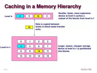
Cache Design • If memory contains 2n addressable words • Memory can be broken up into blocks with K words per block. Number of blocks = 2n / K • Cache consists of C lines or slots, each consisting of K words • C << M • How to map blocks of memory to lines in the cache? Memory Block 0 Block 1 … Block (2n/K)-1 Cache Line 0 Line 1 … Line C-1
Cache Design • Size • Mapping Function • Replacement Algorithm • Write Policy • Block Size • Number of Caches
Size does matter • Cost • More cache is expensive • Speed • More cache is faster (up to a point) • Checking cache for data takes time • Adding more cache would slow down the process of looking for something in the cache
Mapping Function • We’ll use the following configuration example • Cache of 64KByte • Cache line / Block size is 4 bytes • i.e. cache is 16,385 (214) lines of 4 bytes • Main memory of 16MBytes • 24 bit address • (224=16M) • 16Mbytes / 4bytes-per-block 4 MB of Memory Blocks • Somehow we have to map the 4Mb of blocks in memory onto the 16K of lines in the cache. Multiple memory blocks will have to map to the same line in the cache!
Direct Mapping • Simplest mapping technique - each block of main memory maps to only one cache line • i.e. if a block is in cache, it must be in one specific place • Formula to map a memory block to a cache line: • i = j mod c • i=Cache Line Number • j=Main Memory Block Number • c=Number of Lines in Cache
Direct Mapping with C=4 • Shrinking our example to a cache line size of 4 slots (each slot/line/block still contains 4 words): • Cache Line Memory Block Held • 0 0, 4, 8, … • 1 1, 5, 9, … • 2 2, 6, 10, … • 3 3, 7, 11, … • In general: • 0 0, C, 2C, 3C, … • 1 1, C+1, 2C+1, 3C+1, … • 2 2, C+2, 2C+2, 3C+2, … • 3 3, C+3, 2C+3, 3C+3, …
Direct Mapping with C=4 Block 0 Valid Dirty Tag Main Memory Block 1 Slot 0 Block 2 Slot 1 Block 3 Slot 2 Block 4 Slot 3 Block 5 Cache Memory Block 6 Each slot contains K words (e.g. 4 words) Tag: Identifies which memory block is in the slot Block 7
Direct Mapping Address Structure • Address is in three parts • Least Significant w bits identify unique word within a cache line • Next Significant s bits specify which slot this address maps into • Remaining t bits used as a tag to identify the memory block
Direct Mapping Address Structure V D Tag t Line or Slot s Word w • Given a 24 bit address (to access 16Mb) • 2 bit word identifier (4 byte block) • Need 14 bits to address the cache slot/line • Leaves 8 bits left for tag (=22-14) • No two blocks in the same line have the same Tag field • Check contents of cache by finding line and checking Tag • Also need a Valid bit and a Dirty bit • Valid – Indicates if the slot holds a block belonging to the program being executed • Dirty – Indicates if a block has been modified while in the cache. Will need to be written back to memory before slot is reused for another block 14 2 1 1 8
Direct Mapping Example, 64K Cache Main Memory Cache Memory Addr Tag W0 W1 W2 W3 Addr (hex) Data 000000 F1 000001 F2 000002 F3 000003 F4 000004 AB … 1B0004 11 1B0005 12 1B0006 13 1B0007 14 00 F1 F2 F3 F4 0 1 2 3 4 5 .. .. 214-1 1B 11 12 13 14 Line 0 Line 1 Line 1 1B0007 = 0001 1011 0000 0000 0000 0111 Word = 11, Line = 0000 0000 0000 01, Tag= 0001 1011
Direct Mapping pros & cons • Simple • Inexpensive • Fixed location for given block • If a program accesses 2 blocks that map to the same line repeatedly, cache misses are very high – condition called thrashing
Fully Associative Mapping • A fully associative mapping scheme can overcome the problems of the direct mapping scheme • A main memory block can load into any line of cache • Memory address is interpreted as tag and word • Tag uniquely identifies block of memory • Every line’s tag is examined for a match • Also need a Dirty and Valid bit • But Cache searching gets expensive! • Ideally need circuitry that can simultaneously examine all tags for a match • Lots of circuitry needed, high cost • Need replacement policies now that anything can get thrown out of the cache (will look at this shortly)
Associative Mapping Example Block 0 Valid Dirty Tag Main Memory Block 1 Slot 0 Block 2 Slot 1 Block 3 Slot 2 Block 4 Slot 3 Block 5 Cache Memory Block 6 Block can map to any slot Tag used to identify which block is in which slot All slots searched in parallel for target Block 7
Associative Mapping Address Structure Word 2 bit Tag 22 bit • 22 bit tag stored with each slot in the cache – no more bits for the slot line number needed since all tags searched in parallel • Compare tag field of a target memory address with tag entry in cache to check for hit • Least significant 2 bits of address identify which word is required from the block, e.g.: • Address: FFFFFC = 1111 1111 1111 1111 1111 1100 • Tag: Left 22 bits, truncate on left: • 11 1111 1111 1111 1111 1111 • 3FFFFF • Address: 16339C = 0001 0110 0011 0011 1001 1100 • Tag: Left 22 bits, truncate on left: • 00 0101 1000 1100 1110 0111 • 058CE7
Set Associative Mapping • Compromise between fully-associative and direct-mapped cache • Cache is divided into a number of sets • Each set contains a number of lines • A given block maps to any line in a specific set • Use direct-mapping to determine which set in the cache corresponds to a set in memory • Memory block could then be in any line of that set • e.g. 2 lines per set • 2 way associative mapping • A given block can be in either of 2 lines in a specific set • e.g. K lines per set • K way associative mapping • A given block can be in one of K lines in a specific set • Much easier to simultaneously search one set than all lines
Set Associative Mapping • To compute cache set number: • SetNum = j mod v • j = main memory block number • v = number of sets in cache Main Memory Block 0 Block 1 Slot 0 Block 2 Set 0 Slot 1 Block 3 Set 1 Block 4 Slot 2 Block 5 Slot 3
Set Associative MappingAddress Structure Word 2 bit Tag 9 bit Set 13 bit • E.g. Given our 64Kb cache, with a line size of 4 bytes, we have 16384 lines. Say that we decide to create 8192 sets, where each set contains 2 lines. Then we need 13 bits to identify a set (213=8192) • Use set field to determine cache set to look in • Compare tag field of all slots in the set to see if we have a hit, e.g.: • Address = 16339C = 0001 0110 0011 0011 1001 1100 • Tag = 0 0010 1100 = 02C • Set = 0 1100 1110 0111 = 0CE7 • Word = 00 = 0 • Address = 008004 = 0000 0000 1000 0000 0000 0100 • Tag = 0 0000 0001 = 001 • Set = 0 0000 0000 0001 = 0001 • Word = 00 = 0
Two Way Set Associative Example Address 16339C
K-Way Set Associative • Two-way set associative gives much better performance than direct mapping • Just one extra slot avoids the thrashing problem • Four-way set associative gives only slightly better performance over two-way • Further increases in the size of the set has little effect other than increased cost of the hardware!
Replacement Algorithms (1)Direct mapping • No choice • Each block only maps to one line • Replace that line
Replacement Algorithms (2)Associative & Set Associative • Algorithm must be implemented in hardware (speed) • Least Recently used (LRU) • e.g. in 2 way set associative, which of the 2 block is LRU? • For each slot, have an extra bit, USE. Set to 1 when accessed, set all others to 0. • For more than 2-way set associative, need a time stamp for each slot - expensive • First in first out (FIFO) • Replace block that has been in cache longest • Easy to implement as a circular buffer • Least frequently used • Replace block which has had fewest hits • Need a counter to sum number of hits • Random • Almost as good as LFU and simple to implement
Write Policy • Must not overwrite a cache block unless main memory is up to date. I.e. if the “dirty” bit is set, then we need to save that cache slot to memory before overwriting it • This can cause a BIG problem • Multiple CPUs may have individual caches • What if a CPU tries to read data from memory? It might be invalid if another processor changed its cache for that location! • Called the cache coherency problem • I/O may address main memory directly too
Write through • Simplest technique to handle the cache coherency problem - All writes go to main memory as well as cache. • Multiple CPUs must monitor main memory traffic (snooping) to keep local cache local to its CPU up to date in case another CPU also has a copy of a shared memory location in its cache • Simple but Lots of traffic • Slows down writes • Other solutions: noncachable memory, hardware to maintain coherency
Write Back • Updates initially made in cache only • Dirty bit for cache slot is cleared when update occurs • If block is to be replaced, write to main memory only if dirty bit is set • Other caches can get out of sync • If I/O must access invalidated main memory, one solution is for I/O to go through cache • Complex circuitry • Only ~15% of memory references are writes
Cache Performance • Two measures that characterize the performance of a cache are the hit ratio and the effective access time (Num times referenced words are in cache) Hit Ratio = ----------------------------------------------------- (Total number of memory accesses) (# hits)(TimePerHit)+(# misses) (TimePerMiss) Eff. Access Time = -------------------------------------------------------- (Total number of memory accesses)

