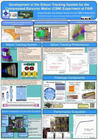
Download
1 / 27
300 likes | 508 Views
Silicon Labs C8051F020 System Overview. Professor Yasser Kadah – www.k-space.org. Recommended Reference. Embedded Programming with Field P rogrammable Mixed Signal Controller , M.T. Chew and G.S. Gupta. C8051F020 System Overview. Introduction C8051F020 system overview

E N D
Silicon Labs C8051F020System Overview Professor Yasser Kadah – www.k-space.org
Recommended Reference • Embedded Programming with Field Programmable Mixed Signal Controller, M.T. Chew and G.S. Gupta.
C8051F020 System Overview • Introduction • C8051F020 system overview • Memory organization • Program and internal data memories • Special function registers • I/O ports • The digital crossbar • 12-Bit analog-to-digital converter • 8-Bit analog-to-digital converter • Digital-to-analog converter • Comparators • Voltage reference for ADC and DAC • Internal voltage reference generator
Microprocessors and Microcontrollers • Microprocessor: general-purpose CPU • Emphasis is on flexibility and performance • Generic user-interface such as keyboard, mouse, etc. • Used in a PC, PDA, cell phone, etc. • Microcontroller: microprocessor + memory on a single chip • Emphasis is on size and cost reduction • The user interface is tailored to the application, such as the buttons on a TV remote control • Used in a digital watch, TV remote control, car and many common day-to-day appliances
Terminology • Integrated Circuit (IC): A miniaturized electronic circuit that consists of semiconductor devices and passive components contained in a package • Central Processing Unit (CPU): This refers to the core of the MCU that executes code • Microcontroller Unit (MCU): This is the standard acronym used for microcontrollers, and refers to the full IC that contains the CPU and peripherals. • “n-bit” – the “n” refers to the data bus width of the CPU, and is the maximum width of data it can handle at a time • Examples: 8-bit MCU, 32-bit MCU
Microcontroller Architectures • Microcontroller architecture refers to the internal hardware organization of a microcontroller • Each hardware architecture has its own set of software instructions called assembly language that allows programming of the microcontroller • Some of the popular microcontroller architectures • Intel 8051 • Zilog Z80 • Atmel AVR
Harvard and von Neumann Architectures • Harvard Architecture—a type of computer architecture where the instructions (program code) and data are stored in separate memory spaces • Example: Intel 8051 architecture • von Neumann Architecture—another type of computer architecture where the instructions and data are stored in the same memory space • Example: Intel x86 architecture (Intel Pentium, AMD Athlon, etc.)
Is 8-bit Still Relevant? • “n-bit” – the “n” refers to the data bus width of the CPU, and is the maximum width of data it can handle at a time • PCs with 64-bit microprocessors are becoming common • Over 55% of all processors sold per year are 8-bit processors, which comes to over 3 billion of them per year! • 8-bit microcontrollers are sufficient and cost-effective for many embedded applications • More and more advanced features and peripherals are added to 8-bit processors by various vendors • 8-bit MCUs are well-suited for low-power applications that use batteries
Introduction to CIP-51 • CIP-51 is the CPU of the Silicon Labs C8051F020 MCU • The CIP-51 implements the standard 8051 organization, as well as additional custom peripherals • At 25 MHz, it has a peak throughput of 25 millions of instructions per second (MIPS) • The CIP-51 has a total of 109 instructions
C8051F020 System Overview • The Silicon Labs C8051F020 is a fully integrated mixed-signalsystem-on-a-chip microcontroller available in a 100-pin package • Mixed-Signal • Contains both digital and analog peripherals • System-on-a-chip (SOC) • Integrates memory, CPU, peripherals, and clock generator in a single package
Memory Organization • The memory organization of C8051F020 is similar to that of a standard 8051 • Program and data memory share the same address space but are accessed via different instruction types
Program Memory • FLASH memory • Can be reprogrammed in-circuit • Provides non-volatile data storage • Allows field upgrades of the 8051 firmware • The C8051F020’s program memory consists of 65536 bytes of FLASH • 512 bytes from addresses 0xFE00 to 0xFFFF are reserved for factory use • 128 bytes at address 0x10000 to 0x1007F (scratchpad memory) can be used as non-volatile storage of program constants
Internal Data Memory • The internal data memory consists of 256 bytes of RAM • The special function registers (SFR) are accessed when the direct addressing mode is used to access the upper 128 bytes of memory locations from 0x80 to 0xFF • The general purpose RAM are accessed when indirect addressing is used to access the upper 128 bytes • The first 32 bytes of the internal data memory are addressable as four banks of 8 general purpose registers • The next 16 bytes are bit-addressable or byte-addressable
Special Function Registers • SFRs provide control and data exchange with the microcontroller’s resources and peripherals • The C8051F020 duplicates the SFRs found in a typical 8051 implementation • The C8051F020 implements additional SFRs which are used to configure and access the sub-systems unique to the microcontroller • This allows the addition of new functionalities while retaining compatibility with the MCS-51 instruction set • The SFRs with addresses ending in 0x0 or 0x8 (e.g. P0, TCON, P1, SCON, IE, etc.) are bit-addressable as well as byte-addressable
I/O Ports • Ports 0, 1, 2 and 3 are bit- and byte-addressable • Four additional ports (4, 5, 6 and 7) are byte-addressable only • There are a total of 64 general purpose port I/O pins • Access to the ports is possible through reading and writing the corresponding port data registers (P0, P1, etc.) • All port pins are 5 V tolerant and support configurable input/output modes and weak pull-ups • In addition, the pins on Port 1 can be used as analog inputs to ADC1
The Digital Crossbar • The digital crossbar is essentially a large digital switching network that allows mapping of internal digital peripherals to the pins on Ports 0 to 3 • This is achieved by configuring the crossbar control registers XBR0, XBR1 and XBR2 • Allows the system designer to select the exact mix of GPIO and digital resources needed for the particular application
12-Bit Analog-to-Digital Converter (ADC0) • On-chip 12-bit successive approximation register (SAR) analog-to-digital converter (ADC0) • 9-channel input multiplexer and programmable gain amplifier • The ADC is configured via its associated special function registers • One input channel is tied to an internal temperature sensor, while the other 8 channels are available externally
8-Bit Analog-to-Digital Converter (ADC1) • On-board 8-bit SAR analog-to-digital converter (ADC1) • Port 1 can be configured for analog input • 8-channel input multiplexer and programmable gain amplifier • The ADC is configurable via its configuration SFRs
Digital-to-Analog Converters • Two 12-bit digital-to- analog converters: DAC0 and DAC1 • The DAC voltage reference is supplied via the dedicated VREFD input pin • The DACs are especially useful as references for the comparators
Comparators • There are two analog comparators on chip: CP0 and CP1 • The comparators have software programmable hysteresis • Generate an interrupt on its rising edge, falling edge or both • The comparators' output state can also be polled in software and programmed to appear on the lower port I/O pins via the crossbar
Voltage Reference for ADC and DAC • A voltage reference has to be used when operating the ADC and DAC • Three external voltage reference input pins: VREF0, VREF1 and VREFD • ADC0 may also reference the DAC0 output internally • ADC1 may also reference the analog power supply voltage (AV+)