Download
1 / 15
150 likes | 317 Views
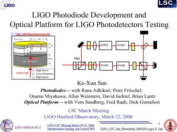
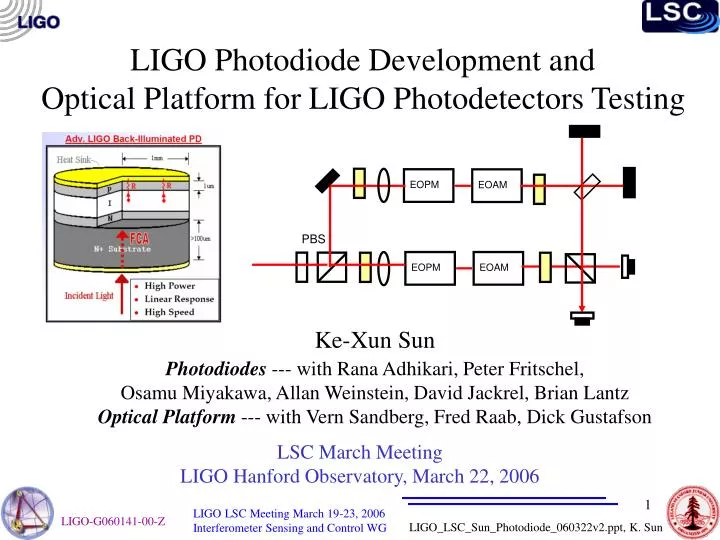
EOPM. EOAM. EOPM. EOAM. LIGO Photodiode Development and Optical Platform for LIGO Photodetectors Testing. PBS. LSC March Meeting LIGO Hanford Observatory, March 22, 2006. Ke-Xun Sun Photodiodes --- with Rana Adhikari, Peter Fritschel,

E N D
EOPM EOAM EOPM EOAM LIGO Photodiode Development and Optical Platform for LIGO Photodetectors Testing PBS LSC March Meeting LIGO Hanford Observatory, March 22, 2006 Ke-Xun Sun Photodiodes --- with Rana Adhikari, Peter Fritschel, Osamu Miyakawa, Allan Weinstein, David Jackrel, Brian Lantz Optical Platform --- with Vern Sandberg, Fred Raab, Dick Gustafson
Material: InGaAs based family Pattern: Single element Diameter > 2 mm Frequency response: ~100 MHz Packaging: rf operable Cooling: Possible TEC Optical power: ~1 W Quantum efficiency target: 70% RF Singlet Detector for LIGO+ and Adv. LIGO 2 mm
Material: InGaAs based family Pattern: Quad (see options right) Gap size > 100 mm Active receiving area: 1 cm2 span Frequency response: >100 MHz Cross talk: 6 dB Better than minimum SNR Neighbor: -20dB @ 100 MHz Diagonal: -23 dB @ 100 MHz Packaging: Multi pin rf operable Optical power: ~100 mW total Quantum efficiency target: 70% Other ideas (see right) RF Quad Detectors for LIGO+ and Advanced LIGO Large gap quad photodiodes Arrayed single detectors Use with lens arrays (commercially available)
Commercial InGaAs Quad Photodiodes • Hamamatsu • 6849-01 • 1 mm, 80 MHz • 6849 • 2 mm, 30 MHz • Cross coupling via the single cathode pin connection A2 A1 C A4 A3
Back Illuminated Photodiodes for High Power Optical Detection • “Flip over” to facilitate heat dissipation • Improved transmittance in the “new front” • Power level raised • Need device packaging • Need RF packaging • Need systematic testing
Probe Testing Results The new 2006 strategy: Packaging and testing needs to be improved for high frequency applications Data shown from D. Jackrel LSC 2005
Catalog existing chips from David Ordered 30 InGaAs chips Negotiating wire bonding RF packaging comparison External resonant elements Structure design to allow TEC cooling Look for a grad student Or an interactive commercial sensor (Commercial products?) Detector Work at Stanford Verify the design first
C1 A2 A1 C2 C4 A3 A4 C3 A4 C4 G4 G3 C3 A3 A1 C1 G1 G2 C2 A2 RF Packaging of Quad Detector Options • Use separate cathode pins • Add grounding ring and grounding for • Better isolation • External resonant circuits • Use BGA pin fan out • Allow heat sink and TEC cooling
PBS BS2 (PBS or NPBS) EOPM EOAM EOPM EOAM EOPM Laser Isolator Optical Test Platform at LIGO HanfordSimulates all field components at all frequenciesCan be built step-by-by step to reduce cost shock
EOAM EOAM Wavefront and Alignment Sensing PZTs Wavefront sensor • RF modulation • Phase • Amplitude • Overlap modulation • Beam displacement (~4x103x(30/2)x10-17~ 0.6 pm) • Coherent (co-polarized fraction) • Incoherent (orthogonal polarized fraction) • Angular modulation Alignment sensor • DC or lock-in amplifier (~100 kHz) frequency LIGO beam pointing simulation PZTs
EOPM Single Side Band Frequency Shift Single side band frequency • Optical heterodyne frequency down shift for advanced LIGO wavefront sensor (Peter Fritschel) • Down shift from 200 MHz to below quad detector bandwidth • No beam movement • Tunable • Double pass AO • Use an acoustic modulator (AO) • Curve mirror • Double pass for 2 w modulation AO
Cavity PBS AO BS2 (PBS or NPBS) EOPM EOAM EOPM EOAM Laser Isolator A More Complete PlatformStep by step implementation • Cavity Phase Shifter • Frequency Shifter
Orthogonally Polarized Local Oscillator • Simulated amplitude noise by using Amplitude modulation • CMRR >30 dB with adjustable gain amplifiers
Spectrum Measurement at 90.9 MHz Amplitude Noise Suppression 32 dBGood for AS_I Mitigation?
SummaryIterative Steps of Detector Development • System requirement • Chipset configuration • Material science • RF packaging • External matching circuit • Device testing • System testing