Download
1 / 29
310 likes | 506 Views
GRAND Perspectives of graphene electronics. Heinrich Kurz Advanced Microelectronic Center Aachen, AMO GmbH Institute of Semiconductor Electronics at RWTH Aachen University. 22 nm. 32 nm. DESIGN. 45 nm. 65 nm. 90 nm. Evolution vs. Revolution of Moore. SETs. Organic Computing.

E N D
GRANDPerspectives of graphene electronics Heinrich Kurz Advanced Microelectronic Center Aachen, AMO GmbH Institute of Semiconductor Electronics at RWTH Aachen University
22 nm 32 nm DESIGN 45 nm 65 nm 90 nm Evolution vs. Revolution of Moore SETs Organic Computing Spintronics Quantenrechner Beyond CMOS More than Moore performance diversification • - ballistic transport • - photonics • - C-interconnects • THz-transistor • non-silicon • graphene • parallel processing • - MEMS • - sensors • - RF • - System-on-Chip • - power electronics • polymer More Moore
Hype Cycles - Gartner Case Study Nanotechnology Valid foranyhighlycompetitivetechnologyfield JT H3 Positive Hype N2B NNI NTD Negative Hype MA+ Take-Off MA SINE STM
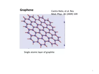
The essence of Graphene Single-layer Graphene Bilayer Graphene H Hamiltonian (Energy), m*effective mass, p momentum vFFermi-velocity, c speed of light, σ Pauli matrices from A.K. Geim, Science 324,1530 (2009)
Carbon and CMOS: 4 - layer problem • Passivation • Exclusion of atmospheric influences Topgate Passivation • Dielectric • Same as for bottom SiO2 • Dielectric constantk • Leakage current • Electrotransport through dielectric Dielectric Graphene Contacts Dielectric (SiO2) • Contacts • Contact resistance • Metall induced doping • Fermi level shift Backgate (Si) Interface SiO2 – Graphene • Interface traps • Surface termination • Bonding • Surface roughness • water • → mobility degradation, doping • Graphene • Relaxed, unrelaxed, strain • p,n puddles • Edge orientation/termination • Unintentional hydrogenation (e.g. HSQ) • Influence of oxygen during etching
GRAND: Overall objectives • Explore the potential of graphene for ICT • Fabrication and simulation of switches (RF, FET, TFET, Sensors) and interconnects at the nanoscale. • Can graphene fulfil its promise of taking CMOS to the “Beyond CMOS” era?
GRAND partners Simulation Device fabrication Coordinator Graphene based FETs and interconnects Simulation Graphene Synthesis Functionalization Characterization
GRAND: Overall objectives Advantages of graphene based devices • High carrier mobility (>10.000 cm²/Vs at RT) • High current carrying capability (>108 A/cm²) • Ultimately thin, ultimate incarnation of the surfaces • p- and n-type behavior nearly symmetric Challenges for realizing graphene based FETs • Introducing a band gap (and preserve carrier mobility) (target: Ion/Ioff>104) • Wafer-scale synthesis of graphene
Graphene FETs • Three concepts for introducing a band gap: • Graphene nanoribbons • Bilayer Graphene with I electric field • Doping of graphene (replacing C-atoms) Experimentally realized yet
Graphene nanoribbons Simulation (TB) of perfect 3.3 nm GNR FETs Na = 28 W = 3.3 nm (Eg = 0.41 eV) doxid = 2 nm ION/IOFF > 104 can be achieved with W = 3.3 nm R. Grassi et al., J. Comp. Elect. 8, 441 (2009)
Graphene nanoribbons GNR fabricated by lithography Source Back-Gate W ~ 20nm Drain • Resistance increases with decreasing T: Energy gap! AMO unpublished
Graphene nanoribbons • Pro: • On/off ratios >104 achievable for w < 4 nm • Contra: • Mobility limited to values < 1.000 cm²/Vs • Edge-roughness dominates transport in devices • Width must be controlled with atomic precision
Bilayer FET Symmetry breaking by vertical E-field introduces gap in bilayer graphene: E-field Two gates required to vary EG and EF
Bilayer FET Consequences for band gap in bilayer graphene: Always a conducting path; band gap not visible in transport.
Scanning gate microscopy Allows local mapping of charge neutrality point M.R. Connolly et al., APL 96, 113501 (2010)
Scanning gate microscopy Variation of the CNP in a graphene flake CNP at gm/G=0 M.R. Connolly et al., APL 96, 113501 (2010)
Bilayer FET Possible solutions: Reducing inhomogenities e.g. by functionalization Patterning to w<~200 nm Realized by CMOS compatible processes
Bilayer FET Bilayer graphene FET w = 50 nm, l = 200 nm B.N. Szafranek et al., APL 96, 112103 (2010)
Bilayer FET Transfer-Characteristics Wolpertinger 1.2 Channel: w = 50 nm l = 200 nm 25 nm SiOx Dmax / ε0 = 1.6 V/nm at UBG = 40V and UTG = -4.5V B.N. Szafranek et al., APL 96, 112103 (2010)
Bilayer FET Characteristic parameters at RT Wolpertinger 1.2 [1] Jiao et al., Nature 458, 877 (April 2009) * EG determined by RDP – D relation
Bilayer FET Bilayer graphene TFET (TB-Simulations) tBG = tTG = 3 nm (SiO2) Emax = 1.3 V/nm • Small slope switches possible with bilayer graphene G. Fiori et al., IEEE Device Lett. 30, 1096 (2009)
Bilayer FET • Pro: • On/off ratios >104 possible with TFETs • Mobility of ~1.000 cm²/Vs already achieved • Mobility > 5.000cm²/Vs possible • Contra: • Device fabrication is more complex
Functionalization • Route for realizing bilayer tunnel FETs: • Further reduction of charge inhomogenities • Advanced dielectric deposition • Controlled doping Functionalization by Tyndall
Functionalization Self assembled monolayer for functionalization of graphene Tyndall to be published
Functionalization Functionalization reduces inhomogenities without annealing Confirmation by scanning gate microscopy needed. Tyndall to be published
Summary • Routes for realizing graphene based FETs • explored theoretically and experimentally: • Graphene nanoribbon FETs show promising on/off • ratios for w<4 nm. • Draw backs: Low mobility and currently not realizable. • Bilayer tunneling FETs are a promising route for low- • power application. • Advantages: Experimentally already realizable and high • mobility.
Thanks to C.G. Smith M.R. Connolly D. Neumaier B.N. Szafranek D. Schall M. Baus S. Roche T. Poiroux F.Triozon • Quinn • B. Long • M. Manning • G. Visemberga Bologna G. Baccarani A. Gnudi E. Sangiorgi S. Reggiani Pisa M. Macucci G. Iannaccone G. Fiori Udine L. Selmi P. Palestri D. Esseni M. Bresciani