Download
1 / 1
10 likes | 146 Views
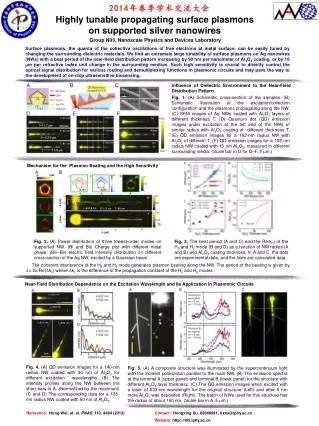
2014 年春季学术交流大会. Highly tunable propagating surface plasmons on supported silver nanowires. Group N03, Nanoscale Physics and Devices Laboratory.

E N D
2014年春季学术交流大会 Highly tunable propagating surface plasmons on supported silver nanowires Group N03, Nanoscale Physics and Devices Laboratory Surface plasmons, the quanta of the collective oscillations of freeelectrons at metal surface, can be easily tuned by changing the surroundingdielectric materials. We find an extremely large tunability of surface plasmons on Ag nanowires (NWs) with a beat period of the near-field distribution pattern increasing by 90 nm per nanometer of Al2O3 coating, or by 16 mm per refractive index unit change in the surrounding medium. Such high sensitivity is crucial to directly control the optical signal distribution for various routing and demultiplexing functions in plasmonic circuits and may pave the way to the development of on-chip ultrasensitive biosensing. Influence of Dielectric Environment to the Near-Field Distribution Pattern. T=0 nm T=50 nm 500 nm Fig. 1. (A) Schematic cross-section of the samples. (B) Schematic illustration of the excitation/collection configuration and the plasmons propagating along the NW. (C) SEM images of Ag NWs coated with Al2O3 layers of different thickness T. (D) Quantum dot (QD) emission images under excitation at the left end of the NWs of similar radius with Al2O3 coating of different thickness T. (E) QD emission images for a 162-nm radius NW with Al2O3 of different T. (F) QD emission images for a 155-nm radius NW coated with 15 nm Al2O3, measured in different surrounding media. (Scale bar in D for D–F, 5 mm.) T=80 nm T=30 nm T=50 nm Air T=30 nm T=55 nm Water T=50 nm T=60 nm Oil T=80 nm Mechanism for thePlasmon Beating and the High Sensitivity l=632.8 nm R=110 nm T=80 nm R = 155 nm Fig. 2. (A) Power distribution of three lowest-order modes on supported NW. (Bi and Bii) Charge plot with different initial phase; (Biii–Bv) electric field intensity distribution on different cross-section of the Ag NW, excited by a Gaussian beam. Fig. 3. The beat period (A and C) and the Re(k//) of the H0 and H2 mode (B and D) as a function of NW radius (A and B) and Al2O3 coating thickness. In A and C, the dots are experimental data, and the lines are calculated data. The coherent interference of the H0 and H2 mode generates plasmon beating along the NW. The period of the beating is given by L= 2p/Re(Dk//) where Dk// is the difference of the propagation constant of the H0 and H2 modes. Near-Field Distribution Dependence on the Excitation Wavelength and Its Application in Plasmonic Circuits l=633 nm 5mm l=532 nm l=633 nm l=532 nm 5mm Fig. 4. (A) QD emission images for a 140-nm radius NW coated with 30 nm of Al2O3 for different excitation wavelengths. (B) The intensity profiles along the NW between the short bars in A. (Normalized by the maximum) (C and D) The corresponding data for a 135-nm radius NW coated with 50 nm of Al2O3. Fig. 5. (A) A composite structure was illuminated by the supercontinuum light with the incident polarization parallel to the main NW. (B) The emission spectra at the terminal A (upper panel) and terminal B (lower panel) for the structure with different Al2O3 layer thickness. (C) The QD emission images when excited with a laser of 633-nm wavelength for the original structure (Left) and after 5 nm more Al2O3 was deposited (Right). The batch of NWs used for this structure has the radius of about 150 nm. (Scale bar in A, 5 mm.) Contact: Hongxing Xu, 82648091, hxxu@iphy.ac.cn Website:http://n03.iphy.ac.cn Reference: Hong Wei, et. al. PNAS 110, 4494 (2013)