Download
1 / 11
110 likes | 212 Views
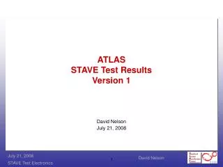
ATLAS STAVE Test Electronics Preliminary V3. Presented by David Nelson. STAVE Test System Block Diagram. POWER. CMD/CLK. CMD/CLK. STAVE INTERFACE BOARD. HOST CPU. USB/ Ethernet. LCLS I/O BOARD. STAVE. DATA. DATA. Communications

E N D
ATLAS STAVE Test ElectronicsPreliminaryV3 Presented by David Nelson
STAVE Test System Block Diagram POWER CMD/CLK CMD/CLK STAVE INTERFACE BOARD HOST CPU USB/ Ethernet LCLS I/O BOARD STAVE DATA DATA • Communications • Host to LCLS board – USB 12Mbit, 10BASE-T, 100BASE-T Ethernet • LCLS I/O board to STAVE interface LVDS CMOS – 160Mbit, 320Mbit • 6 Command, 3 clock signals to STAVE interface • 30 data from STAVE interface, 40 in future • STAVE interface board to STAVE – Differential LVDS – 320Mbit • 6 Command, 3 clock signals to STAVE interface • 30 hybrid channels, easily upgraded to 40 hybrid channels from STAVE interface • Power
LCLS I/O Board using Xilinx FX40 FPGA Configuration Register FSM & CLK 3 USB Or Ethernet Command 0-5 Serializers CMD FIFO 2K*16b USB INTERFACE 6 STAVE INTERFACEBOARD DATA BUFFERS 30*1K*16b Channel 0-29 Deserializers 30 FSM RESET FSM(s) 0-29
STAVE Interface Board – CMOS to LVDS ATCA Connector Connector 3 CLK LVDS 6 STAVE Command LCLS I/O BOARD LVDS Channel Data 30 LVDS Connector Power
XILINX FX40 • 144 each 18Kb memory blocks, we need 32 • Arrangements • 1K * 18b, 2K * 9b, 512 * 36b • Memory can be grouped into larger blocks such as 32Kb without additional logic • FIFO • Random access • 500MHz • PowerPC 405 – Two each • Features • 450MHz • 16KB instruction cache • 16KB data cache • Can be used for such things as histogram processing. • Would not be to process at 160/320MHz clock rates • 448 I/O pins • Built in serializer/deserializer logic in all I/O pins • FF1152 package for FX40, FX60, FX100 • Any of the these three devices can be loaded on board.
LCLS I/O Board Configuration Register • Configuration Register • 32 bits , write/read • Sets STAVE clock frequency • Sets clock polarity for incoming data • Adjust clock delay in 1ns steps for outgoing commands and incoming data • Select data histogram • What other options??
LCLS I/O Board Command FIFO • Command FIFO, Figure 1 • 1K x 32b Maximum • Control Command fields 1, 2, 3 & 5 are encoded into 4 bits • Command field of 0 flags end of buffer • Data field for cal pulse is delay count in clock cycles • Cmd Enable linearly selects any or all Command drivers to STAVE Figure 1
LCLS I/O Board Channel Deserializer(s) 1 K * 16b Histogram Buffer Channel 0 Deserializer Channel 0 * * * * * * * * * * * * * * Channel 0 FSM * * 1 K * 16b Histogram Buffer Channel 29 Deserializer Channel 29 Channel 29 FSM
LCLS I/O Board Channel Histograms • STAVE • Organization • 30 channels • 6 chips per channel • 128 strips per chip • 768 strips per channel • Each strip is assigned one location in the 1K*16b memory • Sequence • Clear all histogram memory buffers • Issue triggers from Cmd FIFO • Read, modify, write each time a hit is found. • This takes 3 clock cycles
LCLS I/O Board Channel Histogram Processing Time calculations for processing 1000 triggers Loading Cmd buffer 2K*16*6MHz = 5mS 6MHz is throughput of USB Executing 1000 triggers @ 40MHz 1000*(35+(64*17*7) )+ 131 = 164mS Readout one 1000 trigger scan 30*768*16*6MHz = 60mS Total time for 1000 triggers is 5mS+164mS+60mS = 229mS Total time for 20 threshold settings is 20 * 229mS = 4.58S