Download
1 / 13
130 likes | 337 Views
New resistive Micromegas electrodes made with sputter deposition. Atsuhiko Ochi Kobe University / MAMMA collaboration. 24/04/2013 RD51 mini week, WG6. Requirements for ATLAS NSW MM. High position resolution for one dimension

E N D
New resistive Micromegas electrodes made with sputter deposition Atsuhiko Ochi Kobe University / MAMMA collaboration 24/04/2013 RD51 mini week, WG6
Requirements for ATLAS NSW MM • High position resolution for one dimension • <100 μm for eta direction.(Resolution of a few cm is allowed for second coordinate.) • Tolerant for high rate HIP particles • ~ 5kHz/cm2 • Resistive layer should be formed as strips • There should be a technology for large size production (~1m) • Mass production should be available • A few thousand board should be produced in 1~2 years. • Low cost is preferable Mesh (GND) +HV A. Ochi, RD51 mini workshop
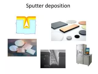
Resistive stripsdeposition Readout strips • Screen printing is used for current prototypes (@ CERN and Japan) • 400 μm pitch was available, but less pitch is very difficult (in our experience) • We have proposed new technique :Sputtering with lift off process • Less than half pitch of readout strips can be formed • We will not need to take care the alignment between resistive strips and readouts.(We have to confirm it) Resistive strips A. Ochi, RD51 mini workshop
Liftoff process using sputtering Photo resist (reverse pattern of surface strips) • Very fine structure (a few tens micro meter) can be formed using photo resist. (same as PCB) • Surface resistivity can be controlled by sputtering material and their thickness @PCB company (Laytech inc.) Substrate (polyimide) Metal/Carbon sputtering @Sputtering company (Be-Sputter inc.) Substrate (polyimide) Developing the resists @PCB company (Laytech inc.) Substrate (polyimide) A. Ochi, RD51 mini workshop
MM PCB production with parallel process • We can divide the production process of resistive strip from that of readout board. • Resistive strip is formed on thin foil • Because of fine pitch, < 200 micron, we don’t need fine alignment between resistive strips and readout strips. • Dividing those processes will make the yield of production growing up. Readout board Resistive Strip foil A. Ochi, RD51 mini workshop
For patterning process: Laytech inc. • PCB company • They are expert for FPC (Flexible Printed Circuit) production. • Liftoff is basic process for FPC production Electro forming machines Etching machines Exposure machines in clean room A. Ochi, RD51 mini workshop
Fine patterning for MPGDs μ-PIC with resistive cathode • Laytech inc has many experiences for producing MPGDs. • μ-PIC with resistive cathode • GEM with resistive foil • MicroMEGAS with screen printing technique 1 mm Bulk MicroMEGASwith screen printingresistive strips 1 mm A. Ochi, RD51 mini workshop
Sputtering process • Sputtering company • They have large sputtering chamber • Φ1800 X H2000 • 1m X 4.5m (flexible board) can be sputtered • They have special technology for uniform sputtering for large area A. Ochi, RD51 mini workshop
Sputtering facilities • Large size sputtering is available. • 4.5m X 1m • Two layer stack sputtering is available • Using two separated target • Very good uniformity • Less than nm size difference, using their special technology Sample Vacuum chamber (with Ar gas) Rotating drum 4.5 m round Sputtering target A. Ochi, RD51 mini workshop
Prototype of resistive foil Carbon (300-600Å) • Tungsten and Carbon are sputtered on polyimide (25μm thickness) foil • Surface resistivity of first sample (W 10Å, C 300Å) was 8MΩ/sq. • Adhesion of coating is very strong. No resistivity change with rubbing surface by cleaning paper. • No resistivity change found after long exposure (1 week) to air Tungsten (10-50Å) Substrate (polyimide) A. Ochi, RD51 mini workshop
Fine patterning with lift off process • Fine strip pitch of 200 μm is formed. It will be possible to make more fine structure. • It keeps strong adhesion and stability A. Ochi, RD51 mini workshop
Mass production feasibility • Assumption: • Size of foils: 1000mm x 500mm • Quantity: 3000 • Sputtering: W:10Å, C:600Å • 500 foils / month can be produced • 8 foils can be sputtered simultaneously in one batch. • Sputtering time is estimated 2 hours.(Including overhead, 3 hours / one batch) • 24h/3h x 8 foils x 20days = 1280 foils / month(Applying safety factor >2 500 foils/month ) • It will take half year, for full production. • Cost estimation (Very rough, but probably upper limit) • Sputtering cost:1k CHF / one batch (for spattering 8 foils)130 CHF / foil ) • It is not sure for the cost of liftoff process, but it is estimated around 200 CHF/foil • Total 330 CHF/foil, 1M CHF for full production Screen printing case (@CERN, by Rui) A. Ochi, RD51 mini workshop
Summary • Resistive electrodes, using sputter technology, are proposed and produced for MPGD production • In our first prototype, surface resistivity is around a 8MΩ/sq., with 10Å tungsten + 300Å carbon. • Very fine (<100 μm) and robust patterns are formed on polyimide foil • Prototype production is taken place at industrial companies Technology transfer is ongoing simultaneously • Both large size production and mass production are available using current facilities • This technique is proposed and tested for MAMMA now, andit will be used for almost all type MPGDs ! A. Ochi, RD51 mini workshop