Download
1 / 24
240 likes | 383 Views
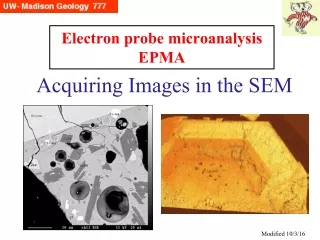
Electron probe microanalysis EPMA. Acquiring Images in the SEM. Modified 10/25/08. What’s the point?. “A picture is worth a thousand words”. The more we know about how images are acquired, the better we can present research results graphically. High Vacuum: Need Conductivity!.

E N D
Electron probe microanalysisEPMA Acquiring Images in the SEM Modified 10/25/08
What’s the point? “A picture is worth a thousand words”. The more we know about how images are acquired, the better we can present research results graphically.
High Vacuum: Need Conductivity! Above left: uncoated. A charge builds up causes oversaturation (white) and horizontal streaking from beam Above right: what same area would appear with conductive coating Right: High vacuum carbon coater (“evaporator” not sputterer)
SEM Resolution Tradition: insert an object with a sharp edge that produces high contrast relative to the background, crank up the mag and measure the distance (red) where the SE (secondary electron) signal changes from 10 - 90% maximum contrast difference. Lyman et al, 1990, “Lehigh Lab Workbook”, Fig 2.2, p. 11
SEM Resolution The above 2 scans show the technique (though apparently the proofreader didn’t catch the inverted signal on the left image). The only way to increase resolution is to turn DOWN the beam current, as the plot on the right shows dramatically -- the current is a few tens of picoamps, not nanoamps. Lyman et al, 1990, “Lehigh Lab Workbook”, Figs A2.3, A2.4, p. 191
SEM Resolution However, the approach apparently used today (e.g. our Hitachi field service engineer) is to take his “test sample” (gold sputtered on graphite substrate) and with optimized contrast, find the narrowest spacing between 2 gold blobs and define that as the “resolution”.
Depth of Field A strength of the SEM is the enhanced depth of field compared to optical microscopy as shown above for the radiolarian Trochodiscus longispinus. Optical image has only a few micron depth of field (=plane in focus), whereas SEM images can be made to be in focus for hundreds of microns (e.g. increasing working distance) Goldstein et al 2003 Fig 1.3
Stigmatism Imperfect magnetic lenses (metal machining, electrical windings, dirty apertures) can cause the beam to be not exactly round, but “astigmatic”. This can be corrected using a “stigmator”, a set of 8 electromagnetic coils. Top left: original “poor” image Top right: underfocus with stig Bottom left: overfocus with stig Bottom right: image corrected for astigmatism. Marker = 200 nm Goldstein et al 2003 Fig 2.24
Edge Effects Edges of objects can appear to be brighter in SE and BSE images, because electrons can be emitted not only from the top but the side, artifically making that part of the image brighter. This can lead to some incorrect conclusions for BSE images. Reed 2005 Fig 4.3
Secondary electron images Everhart-Thornley detector: low-energy secondary electrons are attracted by +200 V on grid and accelerated onto scintillator by +10 kV bias; light produced by scintillator (phosphor surface) passes along light pipe to external photomultiplier (PM) which converts light to electric signal. Back scattered electrons also detected but less efficiently because they have higher energy and are not significantly deflected by grid potential. (image and text from Reed, 1996, p. 37) SE imaging: the signal is from the top 5 nm in metals, and the top 50 nm in insulators. Thus, fine scale surface features are imaged. The detector is located to one side, so there is a shadow effect – one side is brighter than the opposite.
SE1 and SE2 The picture gets a little more complicated … secondary electrons in fact can be generated and detected from more than just the “landing point” of the E0 beam (SE1’s). As the electron scatters away from the impact spot, if it stays near the surface, a second generation (SE2’s) can be generated and detected -- these will cause the SE image to be less sharp. Solution: go to lower E0 (5 kV or less is mentioned by Goldstein) Goldstein et al 2003 Fig 3.20
SE1 and SE2…and SE3! And in the real world it may be even more complicated … backscattered electrons may bounce off the chamber walls, or the bottom of the column, generating SE3’s. Because the E-T detector has a positive bias to attract the low energy SEs, these extraneous signals can add more noise to the image. This is especially problematic at high E0s and is a reason not to expect high resolution SE images at high kV values. Goldstein et al 2003 Fig 4.20
BSE images There are several different types of detectors used to acquire BSE images: Everhart-Thornley detector can have a -50 ev bias put on the grid to reject secondary electrons, so only BSEs get thru -- however this is not useful at fast, TV scanning rates, i.e. moving the stage. Robinson detector — a modern version of the E-T for BSE at TV rates. Must be inserted and retracted. Solid state detector — which is most commonly used today on electron microprobes and many SEMs. Permanently mounted below polepiece. BSE imaging: the signal comes from the top ~.1 um surface). Above, 5 phases stand out in a volcanic ash fragment
BSE images A solid-state (semi-conductor) backscattered electron detector (a) is energized by incident high energy electrons (~90% E0), wherein electron-hole pairs are generated and swept to opposite poles by an applied bias voltage. This charge is collected and input into an amplifier (gain of ~1000). (b) It is positioned directly above the specimen, surrounding the opening through the polepiece. In our SX51 BSE detector, we can modify the amplifier gain: BSE GMIN or BSE GMAX. BSE imaging: the signal comes from the top ~.1 um surface; solid-state detector is sensitive to light (and red LEDs). Goldstein et al, 1992, Fig 4.24, p. 184
There are several alternative type SEM images sometimes found in BSE or SE imaging: (left) channeling (BSE) and (right) magnetic contrast (SE). I have found BSE images of single phase metals with crystalline structure shown by the first effect, and suspect the second effect may be the cause of problems with some Mn-Ni phases. Variations on a theme Crystal lattice shown above, with 2 beam-crystal orientations: (a) non-channeling, and (b) channelling. Less BS electrons get out in B, so darker. From Newbury et al, 1986, Advanced Scanning Electron Microscopy and X-ray Microanalysis, Plenum, p. 88 and 159.
Electron backscatter diffraction is a relatively new and specialized application whereby a specimen (single crystal or more commonly a polished section) is tilted acutely (~70°) in an SEM with a special detector (‘camera’). The electron beam interacts with the crystal lattice and the lattice planes will diffract the beam, with the backscattered electrons striking the detector, yielding sets of intersecting lines, which then can be indexed and crystallographic data deduced. EBSD* * Also referred to as Kikuchi pat-terns. There is a similar phenom-enon, of internally generated x-rays diffracting on the internal structure: Kossel X-ray diffraction. (Left) EBSD pattern from marcasite (FeS2) crystal. (Right) Diagram showing formation of cone of diffracted electrons formed from a divergent point source within a specimen. Dingley and Baba-Kishi, 1990, Electron backscatter diffraction in the scanning electron microscope, Microscopy and Analysis, May.
EBSD “cameras” may have a pair of Si-chip BSE detectors up high, and a pair down low. These lower ones detect high energy electrons that are scattered in a forward direction, with a component of diffraction. They thus give crystallographic orientation information to the image. Here is an image (courtesy Jason Huberty) of a banded iron formation rock from Australia. Forescattered Image The normal BSE image would only show the thin brighter folded bands of magnetite, with the uniformly dark grey quartz. However in the above image, you see each discrete quartz crystal with the grey level indicating a particular orientation. And a careful look at the magnetite show both separate MT domains, plus small lines of pits down the center of each row, whose meaning is being investigated.
BSE and SE Detectors on our SX51 Annular BSE detectors Anti-contamination air jet Plates for +voltage for SE detector View from inside, looking up obliquely (image taken by handheld digital camera)
Annular BSE detector Hitachi SEM Detectors EDS detector ESED detector E-T SE detector IR Chamberscope View from inside, looking up obliquely (image taken by handheld digital camera)
Mosaic Images There are occasions where the feature you wish to image is larger than the field of view acquirable by the rastered beam. A complete thin section (24x48 mm) can have a mosaic BSE image acquired in < 1 hour (though an X-ray map could take a week, so only smaller areas are typically X-ray mapped.) This is achieved by tiling or mosaicing smaller images together. The software calculates how many smaller images are needed based upon the field of view at the magnification used, drives to the center of each rectangle, and then seemlessly stitches the images into one whole. The false colored BSE image of a cm-sized zoned garnet to the right was made by many (>100) 63x scans (each scan 1.9 mm max width). From research of Cory Clechenko and John Valley.
X-ray maps …. And the Clock 3 X-ray maps combined; each element set to a color, and then all merged together in Photoshop. The maps took ~8 hours to collect. Reed, 1996, Fig 6.1, p. 102 X-ray maps can provide useful information as well as attractive ‘eye candy’. However, due to the low count rate of detected X-rays, dwell times generally need to be hundreds of milli-seconds. A 512x512 X-ray map at 100 msecs takes ~8 hours to acquire. Large area maps that combine beam and stage movement require additional ‘overhead’ (~1-10%) for stage activity. The recent improvements to our EDS system give us more leeway, as the larger solid angle of EDS and improved digital processing throughput lets us use 1-10 msec dwell times, as well as allowing low mag images (no need to worry about Rowland circle defocusing).
Image Acquisition Consider: What Image depth?: 8 bit (SE,BSE,CL) or 16 bit (X-ray) -- which translates into: 256 vs 65536 intensity (‘gray’) levels Image size mm in x and y (rectangular vs square; depends on machine/software) pixels in x and y Image resolution-- is it sufficient for the need? mm/pixel + total pixels + final printed size ==> will determine whether or not it is pixelated Image size: total kb or mb. Storage can become an issue when you have lots of large (> 2 mb) images, but with today’s storage options, this is less difficult, as students can afford 250 mb Zip disks. Time for acquisition: SE,BSE,CL is rapid; X-rays require much longer time EDS spectra: sometimes a picture of two contrasting spectra is useful. Adjust conditions (brightness, contrast) for optimal image quality BEFORE you acquire. Be sure not to oversaturate the brightest phases. Record conditions (keV, nA, dwell time, mag) in your lab notebook (scale bar may NOT be necessarily saved on image)
Image Storage Use clear, descriptive names for your images Pick a format for your needs: for ‘plain old images, nothing fancy planned’ JPEG is OK (image size is small) If you know you will be doing some image processing, particularly quantitative, then TIFF is preferable (though images can be very large) Transfer your images to your own computer in a timely manner (they will remain on probe lab computer for a limited period (1-3 years?) Always fiddle with copies, not originals
Some Image Formats JPEG: Name refers to a compression method that is Lossy*: there is some loss of exact pixel values; square subregions are processed with ‘cosine transform’ operation; compression of 10:1 to 100:1 is possible (Joint Photography Experts Group) TIFF: Lossless* compression (image does not degrade with repeated opening/closing). Photoshop gives option of LZW compression, best not used. (Tagged Information File Format) Photoshop (psd): layered image; must flatten if to be used elsewhere. Adobe Acrobat (pdf): non-Lossy compression Graphic Converter (Mac) is a ‘Swiss Army tool’ program that can open about any format you can think of, and save to anything else. (Share/cheapware) Lossy compression throws away some data to better compress the image size; different schemes focus on different features, i.e. JPEG is based on fact that human eye is more sensitive to changes in brightness than in color, and more sensitive to gradations of color than to rapid variations within that gradation. JPEG keeps most brightness info and drops some color info.