Download
1 / 110
1.1k likes | 1.17k Views
This article explores sheet resistance in IC resistors and delves into basic electrical properties of MOS and BiCMOS circuits, with a focus on I-V characteristics and channel length modulation. Learn about pass transistor logic circuits and substrate bias effects.

E N D
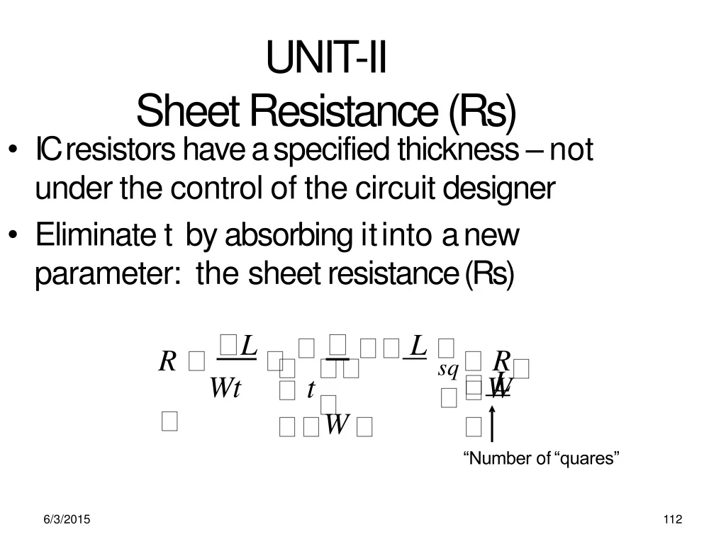
UNIT-IISheet Resistance(Rs) • IC resistors have a specified thickness – not underthecontrolofthecircuitdesigner • Eliminate t by absorbing itinto a new parameter:the sheet resistance(Rs) R LLR L sq Wt W t W “Number of“quares” 6/3/2015 112
BASIC ELECTRICALPROPERTIES • Topics • Basic electrical properties of MOS and BiCMOS circuits: • Ids-Vdsrelationships • MOS transistor threshold voltage, gm,gds • figure of meritwo • passtransistor • NMOSinverter • Various pull-ups • CMOS inverter analysis anddesign • BiCMOSinverters 6/3/2015
MOSFET I-VCharacteristics I-V Plots, Channel Length Modulation -4 x10 – Saturation equation yields curves independentof 6 VGS= 2.5V ResistiveSaturation 5 4 VGS=2.0 V VDS =VGS - VT ID(A) Quadratic Relationship 3 VDS. Not sure!So we consider the effect of channel1 length modulation. 2 VGS=1.5 V VGS=1.0 V 2 2.5 0 0 0.5 1 1.5 VDS(V) 130
MOSFET I-V Characteristics Channel LengthModulation • ChannelLength • Modulation • With pinch-off the channel at thepoint y such that Vc(y)=VGS - VT0, The effective channel length is equal to L’ = L –ΔL • ΔL is the length of channelsegment over whichQI=0. • Place L’ inthe • ID(SAT)equation: VS=0 VDS>VDSAT VGS>VT0 n Cox W( )2 ID(SAT) LV GSV T 0 2 Oxide 0 y L’ΔLL Source n+ Drain n+ (p+) (p+) Channel Pinch-off point(QI=0) Depletionregion Substrate(p-Si) VB=0
MOSFET I-V Characteristics Channel LengthModulation – ΔL increases with an increase inVDS. We canuse 11 L' L ΔL 1 1 1 1 L1V 1 1 L L ΔL 11V ΔL L DS L L 1 – λ: channel lengthmodulation coefficient – ID(SAT) can be rewrittenas DS L – The above form produces a discontinuity of current at VDS=VGS- VT0. We can include the term inID(lin) with little error since λ is typically less than 0.1. We will usually ignore λ in manualcalculations. n Cox W(V V)2(1V) ID(SAT) GS T0 DS 2 L
MOSFET I-V Characteristics Substrate BiasEffect • So far, VSB=0 and thus VT0 used in theequations. • Clearly not always true – must consider bodyeffect – Two MOSFETs inseries: M1 G D S M2 G D VSB S – – – V“B(M1) = VD“(M2) ≠ 0. Thus, VT0 in the M1 equation isreplaced by VT = VT(VSB) as developed in the threshold voltagesection.
MOSFET I-V Characteristics Substrate Bias Effect(Cont.) • The general form of ID can be writtenas • ID = f(VGS,VDS,VSB) • whichduetothebodyeffectterm isnon- linearandmoredifficulttohandleinmanual calculations
MOSFET I-V Characteristics Summary of AnalyticalEquations – The voltage directions and relationships for thethree modes of pMOS are in contrast to those ofnMOS. D B G VSB VDS ID VGS S S V GS VSB B G VDS ID D
Pass-Transistor Logic Circuits(1) • A simple approach for implementing logic functions utilizes series and parallel combinations of switches that are controlled by input variables to connect the input and outputnodes. • Each of the switches can be implemented either by a single NMOS transistor or by a pair of CMOS transistors connected in CMOS transmissiongate configuration. Y=AC 136
Pass-Transistor Logic Circuits(2) • An essential requirement in the design of pass-transistor logic is ensuring that every circuit node has at all times a low-resistance path to VDD or toground. A basic design requirement of PTL circuits is that every node have, at all times, a lowresistance path to either ground or VDD. Such a path does not exist in (a) when B is low and S1 is open. It is provided in 6/3/2015 137 (b) through switchS2.
Pass-Transistor Logic Circuits(3) • The problem can be easily solved by establishing for node Y a low- resistance path that is activated when B goeslow. A basic design requirement of PTL circuits is that every node have, at all times, a lowresistance path to either ground or VDD. Such a path does not exist in (a) when B is low and S1 is open. It is providedin (b) through switchS2.
I-VCharacteristics • In Linear region, Ids dependson • How much charge is in thechannel? • How fast is the chargemoving?
ChannelCharge • MOS structure looks like parallelplate capacitor while operating ininversion • – Gate – oxide –channel • Qchannel= gate Vg + + polysilicon gate Cg Vgd sourceVgs drain W - - - + V V channel s d n+ n+ tox Vds p-type body SiO2 gateoxide L n+ n+ (good insulator, =3.9) ox p-typebody
ChannelCharge • MOS structure looks like parallelplate capacitor while operating ininversion • – Gate – oxide –channel • Qchannel =CV • C= • gate Vg + + polysilicon gate Cg Vgd sourceVgs drain W - - - + V V channel s d n+ n+ tox Vds p-type body SiO2 gateoxide L n+ n+ (good insulator, =3.9) ox p-typebody
ChannelCharge • MOS structure looks like parallelplate capacitor while operating ininversion • – Gate – oxide –channel • Qchannel =CV • C = Cg = eoxWL/tox =CoxWL Cox = ox /tox gate • V= Vg + + polysilicon gate Cg Vgd sourceVgs drain W - - - + V V channel s d n+ n+ tox Vds p-type body SiO2 gateoxide L n+ n+ (good insulator, =3.9) ox p-typebody
ChannelCharge • MOS structure looks like parallelplate capacitor while operating ininversion • – Gate – oxide –channel • Qchannel =CV • C = Cg = eoxWL/tox =CoxWL • V = Vgc – Vt = (Vgs – Vds/2) –Vt Cox = ox /tox gate Vg + + polysilicon gate Cg Vgd sourceVgs drain W - - - + V V channel s d n+ n+ tox Vds p-type body SiO2 gateoxide L n+ n+ (good insulator, =3.9) ox p-typebody
Carriervelocity • Charge is carried bye- • Carrier velocity v proportional to lateralE-field between source anddrain
Carriervelocity • Charge is carried bye- • Carrier velocity v proportional to lateralE-field between source anddrain • v=mEm calledmobility • E=energy 150
Carriervelocity • Charge is carried bye- • Carrier velocity v proportional to lateralE-field between source anddrain • v =mE • E =Vds/L • Time for carrier to crosschannel: • – t= m calledmobility
Carriervelocity • Charge is carried bye- • Carrier velocity v proportional to lateralE-field between source anddrain • v =mE • E =Vds/L • Time for carrier to crosschannel: • – t = L /v m calledmobility
nMOS LinearI-V • Now weknow • How much charge Qchannel is in thechannel • How much time teach carrier takes to cross Ids
nMOS LinearI-V • Now weknow • How much charge Qchannel is in thechannel • How much time teach carrier takes to cross Qchannel I ds t
nMOS LinearI-V • Now weknow • – How much charge Qchannel is in thechannel – HoQw much time teach carrier takes to cross channel t I ds WV V C V Vds 2 gs t ds ox L W L V =C VVVds 2 ox gst ds
nMOS SaturationI-V • If Vgd < Vt, channel pinches off neardrain • – When Vds > Vdsat = Vgs –Vt • Now drain voltage no longer increasescurrent Ids
nMOS SaturationI-V • If Vgd < Vt, channel pinches off neardrain • – When Vds > Vdsat = Vgs –Vt • Now drain voltage no longer increasescurrent V V Vdsat I V 2 ds gs t dsat
nMOS SaturationI-V • If Vgd < Vt, channel pinches off neardrain • – When Vds > Vdsat = Vgs –Vt • Now drain voltage no longer increasescurrent V VVdsat I V 2 ds gst dsat VV 2 gst 2
nMOS I-VSummary • Shockley 1st order transistormodels 0 cutoff Vgs Vt V I V VVds linear V V 2 ds gs t ds ds dsat V Vt 2 saturation Vds Vdsat gs 2
Example • Example: a 0.6 mm process fromAMI semiconductor • – tox = 100Å • – m = 350cm2/V*s • – Vt = 0.7V • Plot Ids vs.Vds • – Vgs = 0, 1, 2, 3, 4,5 • – Use W/L = 4/2l 2.5 Vgs =5 2 1.5 V =4 Ids(mA) gs 1 Vgs =3 0.5 Vgs =2 Vgs =1 0 0 1 2 3 4 5 Vds W3.98.8510 L W L 14 W C A/V 2 350 120 L ox 100108 6/3/2015 160
Vdd Basic Inverter: Transistor with source connected to ground and a load resistor connected from the drain tothe positive Supplyrail R Pull-Up Vo Output is taken from the drain and control input connected between gate andground Resistors are not easily formed insilicon - they occupy too mucharea Vin PullDown Transistors can be used as the pull-updevice Vss
NMOS Depletion Mode Transistor Pull -Up Vdd • Pull-Up is always on – Vgs = 0;depletion D • Pull-Down turns on when Vin >Vt • With no current drawn from outputs,Ids • for both transistors isequal S Vo V0 Vt Vdd D Vin S Non-zerooutput Vss Vi
Ids Vgs=0.2VDD Ids Vgs=0 Vgs=-0.2VDD Vgs=-0.4 VDD Vgs=-0.6VDD VDD–Vds V ds Vin Vgs=VDD VDD Ids Vgs=0.8VDD Vgs=0.6VDD Vgs=0.4VDD Vgs=0.2VDD Vds V o VDD VDD
Decreasing Zpu/Zpd Vin VDD Increasing Zpu/Zpd Vo V DD Vinv • Point where Vo = Vin is calledVinv • Transfer Characteristics and Vinv can be shifted by alteringratio • of pull-up to Pull downimpedances
NMOS Depletion Mode Inverter Characteristics • Dissipation is high since rail to railcurrent flows when Vin = Logical1 • Switching of Output from 1 to0 begins when Vin exceeds Vt of pull downdevice • When switching the output from 1 to 0, the pull up device is non-saturated initially and this presents a lower resistance throughwhich to charge capacitors (Vds < Vgs –Vt)
NMOS Enhancement Mode Transistor Pull -Up Vdd • Dissipation is high since current flows when Vin =1 D • Vout can never reach Vdd (effect ofchannel) • Vgg can be derived from a switching source (i.e. one phase of a clock, so that dissipation can be significantlyreduced Vgg S Vo • If Vgg is higher than Vdd, and extra supply rail isrequired V0 Vdd D Vt (pullup) Vin S Non zerooutput Vss Vt (pulldown) Vin
Cascading NMOSInverters When cascading logic devices care must be taken to preserve integrity of logiclevels i.e. design circuit so that Vin = Vout =Vinv Determinepull–uptopull-downratiofordriveninverter 180
Assume equal margins around inverter; Vinv = 0.5Vdd Assume both transistors in saturation, therefore: Ids = K (W/L) (Vgs – Vt)2/2 Depletion mode transistor has gate connected to source, i.e. Vgs =0 Ids = K (Wpu/Lpu)(-Vtd)2/2 Enhancement mode device Vgs = Vinv, therefore Ids = K (Wpd/Lpd) (Vinv –Vt)2/2 Assume currents are equal through both channels (no current drawn byload) (Wpd/Lpd) (Vinv – Vt)2 = (Wpu/Lpu) (-Vtd)2 Convention Z =L/W Vinv = Vt – Vtd /(Zpu/Zpd)1/2 Substitute in typical values Vt = 0.2 Vdd ; Vtd = -0.6 Vdd ; Vinv = 0.5Vdd This gives Zpu / Zpd = 4:1 for an nmos inverter directly driven by anotherinverter
Pull-Up to Pull-Down Ratio for an nMOS inverterdriven through 1 or more passtransistors Inverter1 Inverter2 Vdd Vdd A B C Vout2 Vin1 It is often the case that two inverters are connected via a series ofswitches (Pass Transistors) We are concerned that connection of transistors in series will degrade the logic levels into Inverter 2. The driven inverter can be designed to deal with this. (Zpu/Zpd>= 8/1)
Complimentary Transistor Pull – Up(CMOS) Vdd Vtn Vtp Vout Pon Noff Non Poff Vo Vin BothOn Vin Vdd Vss Vss Logic1 Logic0
Vtn Vtp Vout 1: Logic 0 : p on ; noff P on Noff Non Poff 5: Logic 1: p off ;n on BothOn 2: Vin >Vtn. Vdsn large – n in saturation Vdsp small – p in resistive Small current from Vdd toVss Vin 4: same as 2 except reversed p andn Vss Vdd 3: Both transistors are insaturation Large instantaneous currentflows 1 2 3 5 4
CMOS INVERTERCHARACTERISTICS n p Current through n-channel pull-downtransistor VDD Vtp Vtn 2 VV n I V n in tn in 2 n 1 p and Vtp =–Vtn Current through p-channel pull-uptransistor If n =p 2 Vtp p I p • VinVDD 2 VDD Vin At logic threshold, In =Ip 2 2 pWp nWn Lp Ln p 2 n Vin Vtn Vin VDD Vtp 2 2 V V V p V V n in tn in DD tp 2 2 Mobilities are unequal : µn = 2.5µp Vin VDD Vtp n Vin Vtn Z =L/W p n n p Vin1 Vtn VDD Vtp p Z/Z= 2.5:1 for a symmetrical CMOSinverter pupd
CMOS InverterCharacteristics • Nocurrentflowforeitherlogical1orlogical0 inputs • Full logical 1 and 0 levels are presented atthe output • For devices of similar dimensions the p– • channel is slower than the n – channeldevice
CMOS InverterVTC NMOS off PMOSres NMOSsat PMOSres 2.5 NMOSsat PMOSsat (V) 2 1.5 Vout 1 0.5 0 NMOSres NMOSres P2M.5OSoff PMOSsat 1.52 0 0.5 1 Vin(V)
Linear Saturation Cutoff Vin -VDD=VGS<VT Vin -Vout=VGD<VT Vin -VDD=VGS>VT Vin-Vout=VGD>VT pMOS Vin -VDD= VGS>VT Vin =VGS>VT Vin -Vout =VGD>VT Vin =VGS>VT Vin -Vout =VGD<VT nMOS Vin = VGS<VT VDD G S Regions ofoperations For nMOS and pMOS In CMOSinverter D Vin D Vout G CL S
Impact of ProcessVariation GoodPMOS BadNMOS (V) 2.5 2 1.5 Vout Nominal 1Bad PMOS 0.5GoodNMOS 0 00.5 1 1.5 2 2.5 • Vin(V) • Pprocess variations (mostly) cause a shift in theswitching • threshold
CmosInverter • Look at why our NMOS and PMOS inverters might not be the best inverterdesigns • Introduce the CMOSinverter • Analyze how the CMOS inverterworks 190
NMOSInverter 5V • When VINchange s to logic 0, itsransistorgets 5V When V is logic 1,V IN OUT logic0. cutoff.ID goes to0. R Constantnonzerocurrent R • ‘esistorvoltagfleowgs othreousghtotraznseisrtoor.. VOUT“pulled uIp=”5/tRo Power is used even though no new computation is being performed. V 5V. D OUT V D OUT D ID =0 VIN 0V VIN 5V + + 5V 0V V DS VDS _ _
PMOSInverter • WhenV5INV changes to logic 1, transistor gets5V cutoff.ID goes to0. V•IN‘esisto-rvoltagegoestozero.VOUVITN“pulled - VDS + down”VtDoS0V V. OUT VOUT + When VIN is logic 0, VOUT is logic1. 0V 5V ID =-5/R 5V ID =0 0V Constant nonzero current flows throughtransistor. Power is used even though no new computation is being performed. R R
Analysis of CMOSInverter • We can foVllow(Lotghice1) same procedure to solvefor DD currents aSnd voltages in the CMOS inverter as wedid for the single NMOS andPMOS circuits. D VOUT • Remember, now we have two transistorsso D we write two I-V relationships and havetwice VIN • the number ofvariables. • We canroSughly analyze the CMOSinverter • NMOSisg“rpaulpl-dhowicnadlelvyic.e” • PMOS is “pull-updevice” • Each shuts off when notpulling
CMOSAnalysis ID(n) As VIN goes up, VGS(n) getsbigger and VGS(p) gets lessnegative. NMOS I-Vcurve PMOS I-V curve (written in termsof NMOSvariables) VIN = VGS(n)= 0.9V VDS(n) VDD