Characterizing InGaAs quantum dot chains
APS 4CS New Mexico Institute of Mining and Technology Socorro, NM October 26-27, 2012. Characterizing InGaAs quantum dot chains. Tyler Park John Colton Jeff Farrer Ken Clark David Meyer Scott Thalman Haeyeon Yang. Outline. Quantum dot (QD) overview

Characterizing InGaAs quantum dot chains
E N D
Presentation Transcript
APS 4CSNew Mexico Institute of Mining and Technology Socorro, NM October 26-27, 2012 Characterizing InGaAs quantum dot chains Tyler Park John Colton Jeff Farrer Ken Clark David Meyer Scott Thalman Haeyeon Yang
Outline • Quantum dot (QD) overview • Quantum dot growth • Photoluminescence (PL) spectroscopy • Transmission electron microscopy • Results
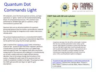
Quantum Dots Overview • QD Overview • QD Growth • PL Spectroscopy • TEM • Results • Charge carriers constrained in 3 dimensions • Quantum well constrained in 1 dimension, quantum wires constrained in 2 • Many uses: optoelectronics, detectors, lasers, quantum computing…
h e- Quantum Dots Overview • QD Overview • QD Growth • PL Spectroscopy • TEM • Results (photon) • Excite electrons across bandgap • “Trap” electrons in well/QD until they relax • Released photons correspond to bandgap energy
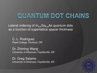
Quantum Dots Overview • QD Overview • QD Growth • PL Spectroscopy • TEM • Results 110 Zh. M. Wang, et al., Journal of Applied Physics, (2006). Dong Jun Kim and Haeyon Yang, Nanotechnology,(2008).
Quantum Dot Growth • QD Overview • QD Growth • PL Spectroscopy • TEM • Results InGaAs • Modified Stranski-Krastanov technique • QD layer grown at a cooler temperature • Annealing process, during which QDs form • Capping layer for electronic/optical uses
Photoluminescence Spectroscopy • QD Overview • QD Growth • PL Spectroscopy • TEM • Results Sample Monochromator Chopper Laser Cryostat Lenses Detector Lock-in Amplifier
Photoluminescence Spectroscopy • QD Overview • QD Growth • PL Spectroscopy • TEM • Results capped, annealed at 460C, 480C, and 500C capped, annealed at 460C
Transmission Electron Microscopy • Preparation: • QD Overview • QD Growth • PL Spectroscopy • TEM • Results Mechanical thinning Scanning electron microscope (SEM) / Focused Ion Beam (FIB)
Transmission Electron Microscopy • QD Overview • QD Growth • PL Spectroscopy • TEM • Results • Cross-sectional and plan view cuts • Analytical transmission electron microscopy (chemical analysis) • Partial electron energy-loss spectroscopy (PEELS) • X-ray energy dispersive spectroscopy (XEDS)
Transmission Electron Microscopy • QD Overview • QD Growth • PL Spectroscopy • TEM • Results
Transmission Electron Microscopy • QD Overview • QD Growth • PL Spectroscopy • TEM • Results
Results and Conclusion • QD Overview • QD Growth • PL Spectroscopy • TEM • Results • Obtained optical and physical information about the quantum dot chains • Found the effect of the capping layer in the quantum dot samples • Investigating quantum dot chain samples with slightly different growth properties • Working with different methods to obtain plan view cuts • Special thanks to: Felipe Rivera, Thomas McConkie, and Richard Vanfleet