Download
1 / 10
100 likes | 118 Views
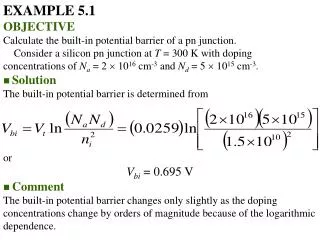
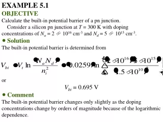
EXAMPLE 5.1 OBJECTIVE Calculate the built-in potential barrier of a pn junction. Consider a silicon pn junction at T = 300 K with doping concentrations of N a = 2 10 16 cm -3 and N d = 5 10 15 cm -3 . Solution The built-in potential barrier is determined from or

E N D
EXAMPLE 5.1 • OBJECTIVE • Calculate the built-in potential barrier of a pn junction. • Consider a silicon pn junction at T = 300 K with doping concentrations of Na = 2 1016 cm-3 and Nd = 5 1015 cm-3. • Solution The built-in potential barrier is determined from or Vbi = 0.695 V • Comment • The built-in potential barrier changes only slightly as the doping concentrations change by orders of magnitude because of the logarithmic dependence.
EXAMPLE 5.2 • OBJECTIVE • Calculate the space charge widths and peak electric field in a pn junction. • Consider a silicon pn junction at T = 300 K with uniform doping concentrations of Na = 2 1016 cm-3 and Nd = 5 1015 cm-3. Determine xn , xp , W , and max . • Solution In Example 5.1, we determined the built-in potential barrier, for these same doping concentrations, to be Vbi = 0.695 V. or xn = 0.379 10-4 cm = 0.379 m The space charge width extending into the p region is found to be or xp = 0.0948 10-4 cm = 0.0948 m
EXAMPLE 5.2 • The total space charge width, using Equation (5.31), is • or • W = 0.474 10-4 cm = 0.474 m • We can note that the total space charge width can also be found from • W = xn + xp = 0.379 + 0.0948 = 0.474 m • The maximum or peak electric field can be determined from, for example, • or • max = 2.93 104 V/cm • Comment We can note from the space charge width calculations that the depletion region extends farther into the lower-doped region. Also, a space charge with on the order of a micrometer is very typical of depletion region widths. The peak electric field in the space charge region is fairly large. However, to a good first approximation, there are no mobile carriers in this region so there is no drift current. (We will modify this statement slightly in Chapter 9.)
EXAMPLE 5.3 • OBJECTIVE • Calculate width of the space charge region in a pn junction when a reverse-bias voltage is applied. • Again, consider the silicon pn junction at T = 300 K with uniform doping concentrations of Na = 2 1016 cm-3 and Nd = 5 1015 cm-3. Assume a reverse-bias voltage of VR = 5 V is applied. • Solution From Example 5.1, the built-in potential was found to be Vbi = 0.695 V. The total space charge width is determined to be or W = 1.36 10-4 cm = 1.36 m • Comment • The space charge width has increased from 0.474 m to 1.36 m at a reverse bias voltage of 5 V.
EXAMPLE 5.4 • OBJECTIVE • Design a pn junction to meet a maximum electric field specification at particular reverse-bias voltage. • Consider a silicon pn junction at T = 300 K with a p-type doping concentration of Na = 1018 cm-3. Determine the n-type doping concentration such that the maximum electric field in the space charge region is max = 105 V/cm at a reverse bias voltage of VR = 10 V . • The maximum electric field is given by • Since Vbi is also a function of Na through the log term, this equation is transcendental in nature and cannot be solved analytically. However, as an approximation, we will assume that Vbi 0.75 V. • We can then write • which yields • Nd = 3.02 1015 cm-3 • We can note that the built-in potential for this value of Nd is • Which is very close to the assumed value used in the calculation. So the calculated value of Nd is a very good approximation. • Comment • A smaller value of Nd than calculated results in a smaller value of max for a given reverse-bias voltage. The value of Nd determined in this example, then, is the maximum value that will meet the specifications.
EXAMPLE 5.5 • OBJECTIVE • Calculate the junction capacitance of a pn junction. • Consider the same pn junction as described in Example 5.3. Calculate the junction capacitance at VR = 5 V assuming the cross-sectional area of the pn junction is A = 10-4 cm2. • Solution The built-in potential was found to be Vbi = 0.695 V. The junction capacitance per unit area is found to be or C = 7.63 10-9 F/cm2 The total junction is found as C = AC = (10-4) (7.63 10-9) or C = 7.63 10-2 F = 0.763 pF • Comment • The value of the junction capacitance for a pn junction is usually in the pF range, or even smaller.
EXAMPLE 5.6 • OBJECTIVE • Determine the impurity concentrations in a p+n junction given the parameters from Figure 5.12. • Consider a silicon p+n junction at T = 300 K. Assume the intercept of the curve on the voltage axis in Figure 5.12 gives Vbi = 0.742 V and that the slope is 3.92 1015 (F/cm2)-2/V. • Solution The slope of the curve in Figure 5.12 is given by 2/esNd , so we canwrite or Nd = 3.08 1015 cm-3 The built-in potential is given by Solving for Na , we find or Na = 2.02 1017 cm-3 • Comment • The results of this example show that Na >> Nd ; therefore the assumption of a one-sided junction was valid.
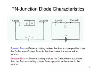
EXAMPLE 5.7 • OBJECTIVE • Determine the diode current in a silicon pn junction dilde. • Consider a silicon pn junction diode at T = 300 K. The reverse-saturation current is IS = 10-14 A. Determine the forward-bias diode current at VD = 0.5 V, 0.6 V, and 0.7 V. • Solution The diode current is found from so for VD = 0.5 V, ID = 2.42 m • and for VD = 0.6 V, • ID = 0.115 m • and for VD = 0.7 V, • ID = 5.47 m • Comment • Because of the exponential function, reasonable diode currents can be achieved even though the reverse-saturation current is a small value.
EXAMPLE 5.8 • OBJECTIVE • Calculate the forward-bias voltage required to generate a forward-bias current density of 10A/cm2 in a Schottky diode and a pn junction diode. • Consider diodes with parameters JsT = 6 10-5 A/cm2 and JS = 3.5 10-11 A/cm2. • Solution For the Schottky diode, we hare Neglecting the (1) term, we can solve for the forward-bias voltage. We find For the pn junction diode, we have • Comment • A comparison of the two forward-bias voltages shows that the schottky diode has an effective turn-on voltage that, in this case, is approximately 0.37 V smaller than the turn-on voltage of the pn junction diode.
EXAMPLE 5.9 • OBJECTIVE • Calculate the space charge width for a Schottky barrier on a heavily doped semiconductor. • Consider silicon at T = 300 K doped at Nd = 7 1018 cm-3. Assume a Schottky barrier with B0 = 0.67 V. For this case, we can assume that Vbi B0. • Solution For a one-sided junction, we have for zero applied bias or xn = 1.1 10-6 cm = 110 Ǻ • Comment • In a heavily doped semiconductor, the depletion width is on the order of angstroms, so that tunneling is now a distinct possibility. For these types of barrier widths, tunneling may become the dominant current mechanism.