Download
1 / 50
510 likes | 728 Views
Learn about the significance of Signal-to-Noise Ratio (SNR) and Noise Factors in measurement systems, including calculations and comparisons at input and output. Explore how Noise Factor (F) is used to evaluate noise contributions and its implications on system performance. Discover insights on Noise Figure (NF) expressed in decibels. References included for further learning.

E N D
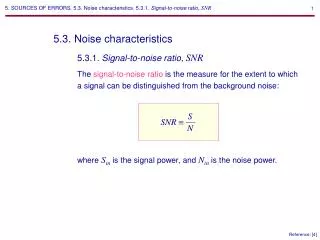
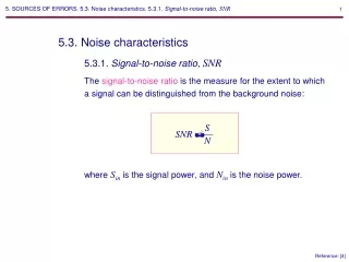
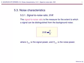
5. SOURCES OF ERRORS. 5.3. Noise characteristics. 5.3.1. Signal-to-noise ratio,SNR 5.3. Noise characteristics 5.3.1. Signal-to-noise ratio,SNR The signal-to-noise ratio is the measure for the extent to which a signal can be distinguished from the background noise: S N SNR . where Smsr is the signal power, and Nmsr is the noise power. Reference: [4] References: [1] and [2]
5. SOURCES OF ERRORS. 5.3. Noise characteristics. 5.3.1. Signal-to-noise ratio,SNR A. Signal-to-noise ratio at the input of the system,SNRmsr Measurement object Measurement system Rs Noiseless Sin Rmsr Smsr Smsr Nmsr SNRmsr . It is usually assumed that the signal power, Smsr, and the noise power, Nmsr, are dissipated in the noiseless input impedance of the measurement system. Reference: [4] References: [1] and [2]
Vin rms2 Rin Rs+ Rmsr 2 1) Smsr= , Vn rms2 Rin Rs+ Rmsr2 2) Nmsr= , Vin rms2 4kTRDfn Vin rms2 Vn rms2 = . 3) SNRmsr= 5. SOURCES OF ERRORS. 5.3. Noise characteristics. 5.3.1. Signal-to-noise ratio,SNR Example: Calculation of SNR at the input of a measurement system Measurement object Measurement system Rs Noiseless Sin Rmsr Smsr
Measurement object Measurement system Rs Noisy SNRo Sin GP Power gain,AP RL 5. SOURCES OF ERRORS. 5.3. Noise characteristics. 5.3.1. Signal-to-noise ratio,SNR B. Signal-to-noise ratio at the output of the system,SNRo So No SNRo . Reference: [4] References: [1] and [2]
Measurement object Measurement system Rs Noiseless SNRo* Sin GP Power gain,AP RL 5. SOURCES OF ERRORS. 5.3. Noise characteristics. 5.3.1. Signal-to-noise ratio,SNR B. Signal-to-noise ratio at the output of the system,SNRo So No* SNRo* . Reference: [4] References: [1] and [2]
Measurement object Measurement system Rs Noisy SNRo Sin GP Power gain,AP RL 5. SOURCES OF ERRORS. 5.3. Noise characteristics. 5.3.2. Noise factor, F, and noise figure,NF 5.3.2. Noise factor, F, and noise figure,NF Noise factor is used to compare at the output the noise contribution of a system (amplifier) against the noise power delivered by the source (H. Friis, 1940s):
SNRo* SNRo SNRmsr* SNRo F = note that SNRo*= SNRmsr*since the measurement system is noiseless. 5. SOURCES OF ERRORS. 5.3. Noise characteristics. 5.3.2. Noise factor, F, and noise figure,NF 5.3.2. Noise factor, F, and noise figure,NF Noise factor is used to compare at the output the noise contribution of a system (amplifier) against the noise power delivered by the source (H. Friis, 1940s): Measurement object Measurement system Rs SNRmsr* Noiseless SNRo* Sin GP Power gain,AP RL
SNRmsr SNRo F . 5. SOURCES OF ERRORS. 5.3. Noise characteristics. 5.3.2. Noise factor, F, and noise figure,NF 5.3.2. Noise factor, F, and noise figure,NF Noise factor is used to compare at the output the noise contribution of a system (amplifier) against the noise power delivered by the source (H. Friis, 1940s): Measurement object Measurement system Rs SNRmsr Noisy SNRo Sin GP Power gain,AP RL
Smsr /Nmsr* So /No (So /AP )/(No*/AP ) So /No = = No No* F , 5. SOURCES OF ERRORS. 5.3. Noise characteristics. 5.3.2. Noise factor, F, and noise figure,NF A. Another definition for noise factor SNRmsr SNRo F where No is the total noise power at the output, and No*is the noise power at the output of the same but noiseless system (the output noise comes only from the source).
5. SOURCES OF ERRORS. 5.3. Noise characteristics. 5.3.2. Noise factor, F, and noise figure,NF Illustration: Measurement object Measurement system Rs Noisy No GP Power gain,AP ens RL
No No* F , 5. SOURCES OF ERRORS. 5.3. Noise characteristics. 5.3.2. Noise factor, F, and noise figure,NF Illustration: Measurement object Measurement system Rs Noiseless No* GP Power gain,AP ens RL
Vno2/RL 4kTRsBn(GVAV)2 /RL = Vno2 4kTRs Bn(GVAV)2 = 5. SOURCES OF ERRORS. 5.3. Noise characteristics. 5.3.2. Noise factor, F, and noise figure,NF Example: Calculation of noise factor Measurement object Measurement system Rs Vmsr Vo GV Voltage gain,AV ens RL No No* F
Vno2 4kTRs Bn(GAV)2 5. SOURCES OF ERRORS. 5.3. Noise characteristics. 5.3.2. Noise factor, F, and noise figure,NF Conclusions: F= The following three characteristics of noise factor can be seen by examining the obtained equation: 1. It is independent of load resistance RL, 2. It does depend on source resistance Rs, 3. If the measurement system were completely noiseless, the noise factor would equal one. References: [2]
Vno2 4kTRs Bn(GAV)2 5. SOURCES OF ERRORS. 5.3. Noise characteristics. 5.3.2. Noise factor, F, and noise figure,NF C. Noise figure Noise factor expressed in decibels is called noise figure(NF): NF 10 log F. Due to the bandwidth term in the denominator there are two ways to specify the noise factor: (1) a spot noise, measured at specified frequency over a 1-Hz bandwidth,or (2) an integrated, or average noise measured over a specified bandwidth. F= References: [2]
5. SOURCES OF ERRORS. 5.3. Noise characteristics. 5.3.2. Noise factor, F, and noise figure,NF E. Measurement of noise factor We will consider the following methods for the measurement of noise factor: (1) the single-frequency method, and (2) the white noise method. 1) Single-frequency method. According to this method, a sinusoidal test signal Vin (rms) is increased until the output power doubles. Under this condition the following equation is satisfied: Measurement object Measurement system Rs Vmsr Vo Vin GV Voltage gain,AV RL References: [2]
Vin=0 Vin=0 Vin=0 Vin=0 2)Vno2=(VinGVAV)2 Vno2 (VinGVAV)2 4kTRs Bn(GVAV)2 No* 3)F= Vin2 4kTRs Bn = = 5. SOURCES OF ERRORS. 5.3. Noise characteristics. 5.3.2. Noise factor, F, and noise figure,NF Measurement object Measurement system Rs Vmsr Vo Vin GV Voltage gain,AV RL 1)(VinGVAV)2+ Vno2=2Vno2 References: [2]
Vin2 4kTRs Bn = 5. SOURCES OF ERRORS. 5.3. Noise characteristics. 5.3.2. Noise factor, F, and noise figure,NF F The disadvantage of the single-frequency meted is that the noise bandwidth of the measurement system must be known. A better method of measuring noise factor is to use a white noise source. 2) White noise method. This method is similar to the previous one. The only difference is that the sinusoidal signal generator is now replaced with a white noise current source: References: [2]
it=0 it=0 it=0 it=0 2)Vno2=(iinRsGAV)2 Bn Vno2 (iinRsGAV)2 Bn 4kTRs Bn(GAV)2 iin2Rs 4kT No* = = 3)F= 5. SOURCES OF ERRORS. 5.3. Noise characteristics. 5.3.2. Noise factor, F, and noise figure,NF Measurement object Measurement system Vin Vo Rs iin(f) GV Voltage gain,AV RL 1)(iin RsGAV)2 Bn+ Vno2=2Vno2
iin2Rs 4kT = 5. SOURCES OF ERRORS. 5.3. Noise characteristics. 5.3.2. Noise factor, F, and noise figure,NF F The noise factor is now a function of only the test noise signal, the value of the source resistance, and temperature. All of these quantities are easily measured. Neither the gain nor the noise bandwidth of the measurement system need be known.
Vno2 4kTRs Bn(GAV)2 5. SOURCES OF ERRORS. 5.3. Noise characteristics. 5.3.2. Noise factor, F, and noise figure,NF D. Limitations of the noise factor concept The concept of noise factor has three major limitations: F= 1. Increasing the source resistance may decrease the noise factor, while increasing the total noise in the circuit. 2. If a purely reactive source is used, noise factor is meaningless, since the source noise is zero, making the noise factor infinite. 3. When the measurement system noise is only a small part of of the source thermal noise (as with some low-noise FETs), the noise factor requires taking the ratio of two almost equal numbers. this can produce inaccurate results. References: [2]
5. SOURCES OF ERRORS. 5.3. Noise characteristics. 5.3.2. Noise factor, F, and noise figure,NF Noise factors varies with the bias conditions, frequency, and temperature as well as source resistance, and all of these should be defined when specifying and comparing noise factors. Knowing the noise factor for one value of source does not allow the calculation of the noise factor at other values of resistance. This is because both the source noise and measurement system noise vary as the source resistance is changed. Noise factor is usually specified for matched devices and is a popular figure of merit in RF applications. References: [2]
en in 5. SOURCES OF ERRORS. 5.3. Noise characteristics. 5.3.3. Two source noise model 5.3.3. Two source noise model A more recent (1956) approach and one that overcomes the limitations of noise factor, is to model the noise in terms of an equivalent noise voltage and current. The actual network can be modeled as a noise-free network with two noise generators, en and in, connected to its input: Measurement object Measurement system Rs Vmsr Vo Noiseless Vin Rmsr AV RL Reference: [2]
en in 5. SOURCES OF ERRORS. 5.3. Noise characteristics. 5.3.3. Two source noise model Measurement object Measurement system Rs Vmsr Vo Noiseless Vin Rmsr AV RL The en source represents the network noise that exists when Rs equals zero, and the in source represents the additional noise that occurs when Rs does not equal zero, The use of these two noise generators plus a complex correlation coefficient completely characterizes the noise performance of the network. At relatively low frequencies, the correlation between the en and in noise sources can be neglected. Reference: [2]
en in 5. SOURCES OF ERRORS. 5.3. Noise characteristics. 5.3.3. Two source noise model Example: Input voltage and current noise spectra (ultralow noise, high speed, BiFET op-amp AD745) Reference: www.analog.com
en in 5. SOURCES OF ERRORS. 5.3. Noise characteristics. 5.3.3. Two source noise model A.Total input noise as a function of the source impedance Measurement object Measurement system Rs Vmsr Vo Noiseless Vin Rmsr AV RL Assuming no correlation between the noise sources, the total equivalent input noise voltage of the whole system can be found by superposition:
en en in Vn in rms = 4kTRsB + Vn rms2 + (In rmsRs)2 . 5. SOURCES OF ERRORS. 5.3. Noise characteristics. 5.3.3. Two source noise model Measurement object Measurement system Rs Vmsr Vo Noiseless Vin Rmsr AV RL Measurement object Measurement system Rs Vmsr Vo Noiseless Vin AV RL in Rs
Vn in 5. SOURCES OF ERRORS. 5.3. Noise characteristics. 5.3.3. Two source noise model We now can connect an equivalent noise generator in series with input signal voltage source to model the total input voltage of the whole system. Measurement object Measurement system Rs Vmsr Vo Vin Voltage gain,AV RL Vn in rms = 4kTRsB + Vn rms2 + (In rmsRs)2 .
100 Vn in in Rs 10 en 4kTRsB Rs Measurement system noise 1 0.1 100 101 102 103 104 Vn in rms = 4kTRsB + Vn rms2 + (In rmsRs)2 . 5. SOURCES OF ERRORS. 5.3. Noise characteristics. 5.3.3. Two source noise model Example: Total equivalent input noise voltage as a function of Rs B = 1 Hz, en = 2 nV/Hz0.5, in = 20 pA /Hz0.5 Vn in rms, nV/Hz0.5 Source noise Rs, W
en en in in Measurement system Noiseless Vn o AV RL Rt 5. SOURCES OF ERRORS. 5.3. Noise characteristics. 5.3.3. Two source noise model B.Measurement of en and in Measurement system Noiseless Vn o en = (Vn o /B) /AV AV RL Vn o rms>> (4kTRt B + Vn2)0.5 in Rs = (Vn o /B) /AV in = (Vn o /B) /AV Rs
en in 5. SOURCES OF ERRORS. 5.4. Low-noise design: noise matching. 5.4.1. Optimum source resistance 5.4. Low-noise design: noise matching 5.4.1. Maximization of SNR Let us first find the signal-to-noise ratio SNR and the noise factor F of the measurement system as a function of the source resistance. We next will try and maximize the SNR at the output of the measurement system by matching the source resistance. Measurement object Measurement system Rs Vmsr Vo Noiseless Vin AV RL
100 Rs for maximum SNR 20 10 10 Vin = en·1 Hz0.5 0 4kTRsB -10 1 Rn forminimum F -20 -30 0.1 F 0.5, dB 100 101 102 103 104 SNR0.5, dB en in Rn= 100 101 102 103 104 5. SOURCES OF ERRORS. 5.4. Low-noise design: noise matching. 5.4.1. Optimum source resistance A.Noise resistance Rn B = 1 Hz, en = 2 nV/Hz0.5, in = 20 pA /Hz0.5 vn in rms = [4kTRs + en rms2 + (in rmsRs)2]0.5 in Rs en vn in rms, nV/Hz0.5 Source noise Measurement system noise en= in Rn Rn is called noise resistance Rs, W
en in SNRmsr SNRo (nVin rms)2 4kTn2Rmsr F = const, SNRmsr= 1 F SNRo= SNRmsr . 5. SOURCES OF ERRORS. 5.4. Low-noise design: noise matching. 5.4.1. Optimum source resistance B.Transformer coupling Measurement object Measurement system Rs Vmsr Vo 1:n Vin AV RL n2Rs nVin
1 F SNRo= SNRmsr 100 20 10 10 Vin = en·1 Hz0.5 0 -10 1 Rn forminimum F -20 -30 0.1 F 0.5, dB 100 101 102 103 104 F Fmin SNR1:n = SNR SNR1: n0.5 SNRmin F 0.5 100 101 102 103 104 5. SOURCES OF ERRORS. 5.4. Low-noise design: noise matching. 5.4.1. Optimum source resistance Example: Transformer coupling B = 1 Hz, en = 2 nV/Hz0.5, in = 20 pA /Hz0.5 Rs 1:n Vin in Rs en vn in rms, nV/Hz0.5 Rs n2 Vin n Source noise 4kTRsB Measurement system noise SNR0.5, dB SNR1:n = n2SNRmin F Rn Rs n2 = Rs, W
en en in in k Noiseless en /in k AV Rs = en /in Rs k = 5. SOURCES OF ERRORS. 5.4. Low-noise design: noise matching. 5.4.1. Optimum source resistance C.Parallel connection of input stages Measurement system Measurement object Rs Vmsr Vo Noiseless Vin AV RL en k /in k=en k 0.5/in k 0.5
5. SOURCES OF ERRORS. 5.4. Low-noise design: noise matching. 5.4.1. Optimum source resistance Example:
en en en 5. SOURCES OF ERRORS. 5.4. Low-noise design: noise matching. 5.4.1. Optimum source resistance D.SNR of cascaded noisy amplifiers Our aim in this Section is to maximize the SNR of a three-stage amplifier. For the sake of simplicity, let us assume that all the stages are identical in terms of noise, and their en>> inRs. Rs Vo AV 1 AV 2 AV 3 Vin Reference: [4]
en en Vin2 /B (4kTRs+en2) + en2/AV12 + en2/AV12AV22 en 3) SNRin 5. SOURCES OF ERRORS. 5.4. Low-noise design: noise matching. 5.4.1. Optimum source resistance Rs Vo AV 1 AV 2 AV 3 Vin Vin2 Vno2/AV12 AV22 AV32 1) SNRin 2) Vno rms2= [(4kTRs+en2)AV12 AV22 AV32 + en2 AV22 AV32 + en2 AV32 ]B Conclusion: keep AV1> 5 to neglect the noise contribution of the second and third stages. Reference: [4]
ID ID rd rd end kT qID ind 1) rd 5. SOURCES OF ERRORS. 5.4. Low-noise design: noise matching. 5.4.2. Noise in diodes 5.4.2. Noise in diodes ID kT q rd , ID= 2) in d 2= 2qID = 2kT/ rd 3) en d 2= (2kT/ rd )rd 2 = 2kT rd
enb inb inc 5. SOURCES OF ERRORS. 5.4. Low-noise design: noise matching. 5.4.3. Noise in bipolar transistors 5.4.3. Noise in bipolar transistors A.Small-signal equivalent circuit Cm rb IB IC vp gmvp B Cp C rp ro enb2= 4kTrb inb2= 2qIB inc2= 2qIC
enb inb inc 5. SOURCES OF ERRORS. 5.4. Low-noise design: noise matching. 5.4.3. Noise in bipolar transistors B.Mid-frequency noise model Rs rb B C gmvp vp Rs in o rp
enb 1) in o2= {[enb rp/(rb+rp )]gm}2 +[ inb (rbIIrp)gm]2 + inc 2 Rs=0 Rs=0 Rs=0 2) in o2= ( inb rpgm)2 + inc 2 inb inc Rs 3) en= in o /Gv Ag , Gv = rp/(rb+ rp), Ag = gm 4) in2= in o /Gi Ag 2 , Gi = rp 5. SOURCES OF ERRORS. 5.4. Low-noise design: noise matching. 5.4.3. Noise in bipolar transistors rb B C gmvp vp Rs in o rp
enb inb inc 5. SOURCES OF ERRORS. 5.4. Low-noise design: noise matching. 5.4.3. Noise in bipolar transistors rb B C gmvp vp Rs in o rp 5) en2= enb2+ (inb rb)2 +[inc(rb+rp )/gm rp ]2 6) in2= inb2+ [inc/(gm+rp )]2
rb B C en en gmvp vp Rs in o rp in in IC IB 5. SOURCES OF ERRORS. 5.4. Low-noise design: noise matching. 5.4.3. Noise in bipolar transistors 5) en2= enb2+ (inb rb)2 +[inc(rb+rp )/gm rp ]2 6) in2= inb2+ [inc/(gm+rp )]2
en in 5. SOURCES OF ERRORS. 5.4. Low-noise design: noise matching. 5.4.4. Noise in FETs 5.4.4. Noise in FETs The noise in bipolar transistors are: - due to the thermal noise of the base resistance, - the shot noise in both the collector and base currents, - and the flicker noise of the base current: BJT en2= 4kTrB+ 2qICre2 in2 = 2qIB + aAIB /f ID IG
5. SOURCES OF ERRORS. 5.4. Low-noise design: noise matching. 5.4.5. Noise in differential and feedback amplifiers 5.4.5. Noise in differential and feedback amplifiers .
5. SOURCES OF ERRORS. 5.4. Low-noise design: noise matching. 5.4.6. Noise measurements 5.4.6. Noise measurements .
J (JFET) FID flicker noise RD thermal noise associated with RD RG thermal noise associated with RG RS thermal noise associated with RS SID shot noise TOT total noise M (MOSFET) FID flicker noise RB thermal noise associated with RB RD thermal noise associated with RD RG thermal noise associated with RG RS thermal noise associated with RS SID shot noise TOT total noise Next lecture Next lecture: D (diode) FID flicker noise RS thermal noise associated with RS SID shot noise TOT total noise
Next lecture Next lecture: J (JFET) FID flicker noise RD thermal noise associated with RD RG thermal noise associated with RG RS thermal noise associated with RS SID shot noise TOT total noise
Next lecture Next lecture: M (MOSFET) FID flicker noise RB thermal noise associated with RB RD thermal noise associated with RD RG thermal noise associated with RG RS thermal noise associated with RS SID shot noise TOT total noise
Next lecture Next lecture: Q (BJT) FIB flicker noise RB thermal noise associated with RB RC thermal noise associated with RC RE thermal noise associated with RE SIB shot noise associated with base current SIC shot noise associated with collector current TOT total noise