GEM foil and Simulation work at CIAE
220 likes | 376 Views
GEM foil and Simulation work at CIAE. Xiaomei Li Shouyang Hu, Jing Zhou, Chao Shan, Siyu Jian and Shuhua Zhou Science and Technology on Nuclear Data Laboratory China Institute of Atomic Energy Solid_gem group meeting. SoLID spectrometer @Jlab 12 GeV. Transversity PVDIS

GEM foil and Simulation work at CIAE
E N D
Presentation Transcript
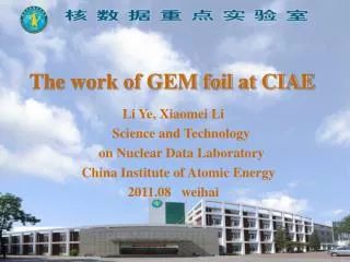
GEM foil and Simulation work at CIAE Xiaomei Li Shouyang Hu, Jing Zhou, Chao Shan, Siyu Jian and Shuhua Zhou Science and Technology on Nuclear Data Laboratory China Institute of Atomic Energy Solid_gem group meeting
SoLID spectrometer @Jlab 12 GeV Transversity PVDIS Longitudinal …
GEM (Gas Electron Multiplier) Structure Core part: GEM Foil Avalanche happens in the hole area only. This improves the spatial resolution in a large extent. Triple-Foil GEM Detector 2012-07-18 KITPC, Beijing, China 4
GEM Foil Structure Typical GEM Foil has 3 layers, two 5μm thick copper foils and one 50μm thick kapton foil in the middle. Diameter of the hole is 70 μm , and the distance between them is 140 μm . Apply electric voltages on the two copper layers. Electric Field is very strong in the hole area, and weak outside the hole area. GEM Foil GEM Field 5 2012-07-18 KITPC, Beijing, China
CIAE has signed officially the LICENSE AGREEMENT FOR MANUFACTURING AND COMMERCIALISATION OF GEM FOILS AND GEM-BASED PRODUCTS with CERN. I took a training for GEM foil at CERN. GEM License and Training
Process Flow Diagram of GEM Foil Manufacture Raw foils 2. Preparing photo mask Lamination and exposure of dry film photoresist 4. Copper etching 5. Kapton etching Second masking, etching and final cleaning Clean room is needed.
Clean Room The cleanrooms at China Institute of Atomic Energy are ISO Class 6.
GEM Photo Mask Plate 10cm*10cm mask plate
The Equipments for Lamination and Exposure of Dry Film Photoresist 1 Lamination and exposure of dry film photoresist are the most important and difficult steps for GEM foil production. We have established a yellow light zone, and have introduced Hot Roll Lamination (HRL) machine and Exposure system. . 2 3
Lamination of Dry Film Photoresist The photoresist is sandwiched between an inner polyolefin cover sheet and an outer Mylar protective layer.
Exposure of Dry Film Photoresist We use negative photoresist for GEM image transfer, unexposed areas are relatively unchanged and easily washed out by solvents during the development. To obtain an identical copy of the photo-mask to the photoresist, vertical sidewalls in the resist are important.
Copper Etching • The solution used to copper etching consists of water, ferric chloride and hydrochloric acid. • Generally the holes in the resist of standard GEMs are 50 µm of diameter. The favored diameter of holes at copper layer is 70 µm with a pitch of 140 µm. Remove photoresist after copper etching
Process flow diagram of GEM Foil Manufacture Purchasing raw materials 2. Preparing photo mask Lamination and exposure of dry film photoresist 4. Copper etching 5. Kapton etching Second masking, etching and final cleaning Clean room is needed.
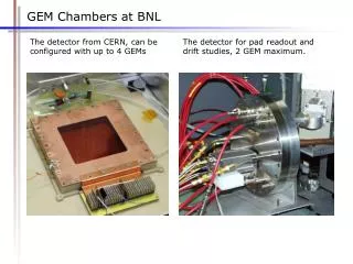
The Status of APV25 Test at CIAE Small APV readout system at CIAE has been installed. There are some problems with DAQ , and we are debugging the software GEM detector (10 cm x 10 cm) is ready for testing.
Calculation Neutron Transfer Efficiency with Geant4 • Simulate the GEM Foil without holes • GEM Foil Size-10X10 cm2 • Boron-10 Coated on both sides of the GEM-foil • Incoming Neutron energy is 0.0254ev • The work gas is Ar/CO2 (80%/20%)
Efficiency VS Number of Boron-GEM Foils We believe with more Boron-GEM Foils, the Neutron Transfer Efficiency will be higher. Boron Thickness is 2.1um
Next step Do more lamination and exposure of dry film photoresist, copper etching to find the best work condition. 2. Finish kapton etching. 3. Test APV25 electronics. 4. Simulation on Neutron Photography with GEM.
Wish to show a prototype of 30*30cm2 GEM foil at the meeting next year! Thank you !