Download
1 / 12
120 likes | 218 Views
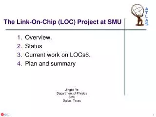
The Link-On-Chip (LOC) Project at SMU. Overview. Status Current work on LOCs6. Plan and summary. Jingbo Ye Department of Physics SMU Dallas, Texas. ADC data. 6. LOCld. VCSEL. MUX. LOCs6. 12-way fiber ribbon. ADC data. LOCld. VCSEL. MUX. LOCs6. Overview (1).

E N D
The Link-On-Chip (LOC) Project at SMU Overview. Status Current work on LOCs6. Plan and summary Jingbo Ye Department of Physics SMU Dallas, Texas
ADC data 6 LOCld VCSEL MUX LOCs6 12-way fiber ribbon ADC data LOCld VCSEL MUX LOCs6 Overview (1) • The Link-on-Chip (LOC) is a concept we proposed for the upgrade of ATLAS/LArFEB optical link which require 100 Gbps/FEB, a 62× increase in data bandwidth. • The ASIC technology has been chosen to be a 0.25 μm silicon-on-sapphire CMOS technology which is commercially available and has MWP runs ~ 6 times a year. • Over time the concept of the transmitting side of the 100 Gbps link has been evolved to be: • We plan to use Serdes-embedded FPGAs for the receiving side of the link and benefit from the developments in the Versatile Link common project especially in optical interface and system design. • The most challenging part in this link is the serializer LOCs6. LOCs6will be a 6-lane array serializer with redundancy switches. Each serializer needs to run at 10 Gbps. Opto WG, TWEPP 2010, Aachen
Overview (2) • To check the serializer design, and to probe the highest speed possible with this technology, we submitted a prototype chip last August 2009. In this 3 mm × 3 mm tile, we have the following designs: • LOCs1, a 5 Gbps 16:1 serializer. • The LCPLL, a 5 GHz LC VCO based phase locked loop. • A standalone CML driver, a copy of that used in LOCs1 • A divide-by-16 circuit. • A varactor, a voltage controlled capacitor. • An SRAM block, designed by Valentino and Mauro. 3 mm 3 mm Opto WG, TWEPP 2010, Aachen
Test results of LOCs1 (1) Opto WG, TWEPP 2010, Aachen
Test results of LOCs1 (2) • Based on 7 boards, power: 463 ±13 mW @ 5Gbps • Jitter tolerance checked • TID and SEE checked with 200 MeVProton. • For more detailed tests please see Datao’s talk. Opto WG, TWEPP 2010, Aachen
Pan to use 2 LOCs6 chips with a 12-way fiber ribbon per FEB. Each chip has an array of six 16:1 serializers, each running at 10 Gbps. One of the six serializers can be configured as a redundant channel. The clock unit will be shared by the serializers to reduce the power. • Next version — LOCs6
10 Gbps 16:1 serializer design diagram The key components needed to be redesigned: 1. 5 GHz LCPLL, LC VCO 2. CML driver for 10 Gbps 3. 2:1 MUX @ 5GHz • 5 GHz Divider • Clock buffer • The core part of this serializer has same architecture as LOCs1. • A few components need to be redesigned for 5 GHz operation frequency. • We choose to use CML circuit for its low noise and high speed performance.
Tuning range: 4.7 to 5 GHz. Expected: 3.79 to 5.01 GHz. Cause traced to the divider in PLL and will fix in the next design. Power consumption: 121 mW Compare: Ring oscillator based PLL, 173 mW at 2.5 GHz Random jitter: 1 - 2.5 ps (RMS) Deterministic jitter:< 17 ps (pk-pk) • 5 GHz LC PLL Fabricated in the same die as LOCs1 is a 5 GHz LC PLL output clock locks to input clock The LC PLL will be used in the 10 Gbps serializer with two changes: Slightly adjust the frequencyso that the center frequency is 5 GHz. Fix the bug in the divider.
Bandwidth: 5 GHz Data rate: up to 8.5 Gbps Plan to use inductive peaking to boost its bandwidth for 10 Gbps data transmission • CML driver We have tested a separate CML driver on the die, same design as used in LOCs1: CML driver test schematic
Swing > 200 mV Freq > 5 GHz Power: ~8 mW Two stage design Fan out two identical buffer without signal attenuation • High speed CML circuit design We designed a CML buffer for 5 GHz clock fan-out. More CML circuit components are ongoing. Parameters for the CML buffer: Schematic and Layout of the CML buffer
CML buffer Post-layout simulation V(v) Output Gain Input V(v) 5 GHz time (ns) Frequency (Hz) Input and output of CML buffer at typical corner and room temperature Frequency response at different temp and corners • CML buffer fans out two identical buffer above 5GHz at different corners and temperature based on post-layout simulation 11
The design of LOCs6 is our main work in the remainder of 2010 and in 2011. As of the LOC1 tests, more will be needed. More tests on LOCs1 are still needed and on-going. First proton test on LOCs1 produced very good results. More tests may be needed to further study the SEE. The success on LOCs1 increased our confidence on LOCs6. We also would like to investigate an array laser driver, LOCLD6, in the same time frame of LOCs6, if possible. We are extremely limited by manpower and resource. We need help in the development of the 100 Gbps/board link system. Collaboration is highly welcome. • Plan and Summary