Download
1 / 38
470 likes | 1.69k Views
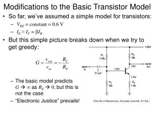
Small Signal Model PNP Transistor. Section 4.4. BJT in the active region. Electrons cross the forward biased BE junction and are swept reverse biased BC junction. Large Signal Model of a BJT. Called “large” signal model because this model is applicable even if V BE

E N D
Small Signal ModelPNP Transistor Section 4.4
BJT in the active region Electrons cross the forward biased BE junction and are swept reverse biased BC junction.
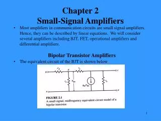
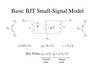
Large Signal Model of a BJT Called “large” signal model because this model is applicable even if VBE changes from 300 mV to 800 mV
Transconductance If a signal changes the base-emitter voltage by a small amount, how much change is produced in the collector current?
But there is something else…. A change in VBE creates a change in base current!
Example 4.10 Signal Generated By a microphone Small Signal Equivalent Circuit VBE=800 mV β=100 IS,Q1=3 x 10-16 A Question: If a microphone generates a 1 mV signal, how much change is observed in the collector and base current?
A Simple Amplifier Determine the output signal level if the microphone produces a 1 mV signal.
AC Ground • The voltage produced by a voltage source is constant. • The small signal model is concerned only with changes in quantities. • Therefore, a DC voltage source must be replaced with a ground in small signal analysis.
Early Effect A larger reverse bias voltage leads to a larger BC depletion region. The effective base width (WB) is reduced. The slope of the electron profile increases. IC increases as VCE is increased.
Assumption • Assume that • The DC at Vout is 0.9 V • gm=1 mS Gain is approximately equal to –gmRC. Bias current is IC=gmVt R=(1.8V-0.9V)/26uA=34.6 Kohms Gain is -34.6.
Peak to Peak Voltage=67.78 mV 67.78 mV/2=33.9
Structures of BJT Transistors (NPN transistor) (PNP transistor)
Voltage and Current Polarities of NPN and PNP transistors A “fat” voltage between collector and emitter voltage places a transistor in the active region! A “skinny” voltage between collector and emitter voltage places a transistor in the active region!
Large-Signal Model of BJT Transistors (NPN) (PNP)
Small Signal Model of BJT Transistors (NPN) (PNP)