Download
1 / 27
270 likes | 306 Views
Characterization of irradiated silicon structures by microwave absorption techniques. E.Gaubas, J. Vaitkus. OUTLINE Motivation of direct control of carrier decays Measurement regimes: MWA/R - slit antenna, MWR - coaxial cable needle probe Evaluation of carrier decay parameters

E N D
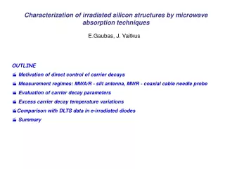
Characterization of irradiated silicon structures by microwave absorption techniques E.Gaubas, J. Vaitkus • OUTLINE • Motivation of direct control of carrier decays • Measurement regimes: MWA/R - slit antenna, MWR - coaxial cable needle probe • Evaluation of carrier decay parameters • Excess carrier decay temperature variations • Comparison with DLTS data in e-irradiated diodes • Summary
Why lifetime direct control? • In the irradiated material different types of defects appear: some of them are important in formation of the space charge, while other are prone to transform and “wait” to become active • Control of the defect types in the sample can be performed by using the direct methods by stimulating defect manifestation, varying measurement regimes and the most important external factors, e.g. exc, BI, T, Iexc etc. • The light pulse is a mean to force the defect system to react and the conductivity change can be detected. • Any change of the system of defects can be revealed: the main difficulty is to interpret the situation, e.g. whether there is transform of traps or a new channel of competition between traps and recombination centers. • Our activities - to design the instruments for analysis of peculiarities of photoresponse and to suggest the methods of extracting the valuable information from the measurement data.
Motivation of non-invasive direct transient techniques ☼ PC measurements can be implemented by using contacts (TCT) or by contact-less probe - microwaves. ☼ Contacts and polarization of sample under bias involve additional problems. Microwave methods are free of contact problems, thus, enabling one to examine the decay temperature variations in order to extract the activation energy of the recombination and trappingcenters, to correlate with parameters estimated by electrical methods as DLTS. ☼The non-invasive contact-less methods can be implemented by using distant measurements, thus, can be applied to control the parameters of detector material just after the irradiationor evenduring irradiation.
Microchip laser STA-01 exc ~700ps, Eexc 10 J M B tiltas MW oscillator with adjustable power and frequency Analyser of the recombination parameters Attenuator of light density Sliding short sample MW slit antenna Sliding short MW bridge M B tiltas Sliding short M MW circulator B cir k ulator ius ³ ³ f f 0.5 0.5 GHz, GHz, £ £ U U 1 mV/pd 1 mV/pd MW detector Amplifier (>50) TDS-5104 Rload
Round Robin calibration of the MWR instruments by using Ge, Si SiPhoenicon (Germany), Si, GePhoenicon-Amecon (IMEC, Belgium), Si, Ge Semilab WT-85X (Umicore, Belgium) Si, GeVUTEG-2 Vilnius
Samples and irradiations ☼Samples investigated for inter-instrument carrier lifetime calibration: I.1. MCZ Si sample 2055 mm3 with two surfaces polished. This sample of about 6 kOhm cm resistivity is mounted with load resistor for simultaneous control of contact photoconductivity. I.2. Phosphorous doped Cz Si 2055 mm3 sample with two surfaces polished. I.3. Phosphorous doped Cz Si 5 mm thick half-wafer with polished surfaces. I.4. Borum doped Cz Si Cz Si 555 mm3 sample with two surfaces polished. I.5. Borum doped Cz Si 5 mm thick half-wafer with polished surfaces. I.6. MCZ n-Si wafer piece of 20200.28 mm3 dimensions. Surfaces are passivated by thermal oxidation. I.7. N-type Ge 352-3 wafer of 500 µm thickness with polished, varnish passivated surfaces. I.8. P-type Ge 327-4 wafer of 500 µm thickness with polished, varnish passivated surfaces. ☼ high resistivity MCZ and FZ silicon wafers and diode structures ☼irradiated by high energyelectrons, -rays, and protons
Measurement instruments available at VU: MWA & MWR - slit antenna, MWR - coaxial needle-tip probe, DLS-82 MW cable laser MWR 22 GHZ probe MWA 10 GHZ probe slit antenna probes Microwave coaxial needle-tip antenna probe
Laser Thermo-couple Tektronix TDS-5104 Cryo-chamber sample in vacuum MW cable Fiber excitation MW cable Cryo-chamber Fiber excitation Cryogenic microwave needle tip -antenna probe integrated with the fiber excitation probe MWR transient variations with temperature in Si diode irradiated with electrons of fluence 3*1012 e/cm2
Blackmore recombination-trapping capt R emis trns Different e & h decay lifetimes, while the effective lifetime is the longest of capt, trns, emis Dominant single level Low defect concentration High defect density S-R-H Carrier pair decay lifetime R, S-R-H=[cp(n0+nex+NCe-(Ec-Em)/kT)+ cn(p0+nex+NV e -(Em-Ev)/kT )]/[n0+p0+nex] g, S-R-H>>R, S-R-H g, S-R-H=[cpNCe-(Ec-Em)/kT+ cnNV e -(Em-Ev)/kT ] sR, S-R-H= snsp[n0s+p0s+nexs ]/[sn(n0s+nexs+Nit,ce-(Ec-Eit)/kT)+ sp(p0+nex+NVit e -(Eit-Ev)/kT )] sg, S-R-H<< sR, S-R-H sg, S-R-H= snsp/[snNit,ce-(Ec-Eit)/kT+ spNVit e -(Eit-Ev)/kT ] sn,p =n,p svNit=n,p sv kT Dit
System of recombination-trapping centers Ryvkin’ model System of recombination centers with different rates Lashkarev’ model capt emis Rslow Ktr R RR Sfast Carrier decay instantaneous lifetime inst=RKtr R(1+ gen/capt) Carrier decay instantaneous lifetime inst=- n/(dn/dt) (ASe-t/s+ ARe-t/R)/(S-1 ASe-t/s + S-1 ARe-t/R ) System of two competing levels
Systems of recombination centers Rose’ model TA R I I R TD S Inter-trap recombination K.Takarabe, P.T.Landsberg, J.K.Liakos. Semic. Sc.Techn.(1997) W.M.Chen, B.Monemar, E.Janzen, J.L.Lindstrom. Phys.Rev.Lett. (1991) Carrier decay instantaneous lifetime photoconductivity quenching etc. qualitative analysis Systems of competing levels Systems of recombination centers W.M.Chen, B.Monemar, E.Janzen, J.L.Lindstrom &Watts’ model
Carrier escape and motion barriers Ec TD Si TD1++e TD1*+e+h ED ED MS: S* TD12++2e EB S TD1o TD1* 0.47 eV B R 0.15 eV A 0.07 eV CC Ev T T 0.48 eV A B CC Extended defects: clusters, SiOx precipitates, disorder etc. G.Pfister,H.Sher Adv.Phys1978), P.T.Landsberg. Rec. Semic.(1991), S.Havlin, D.Ben-Avraham. Adv. Phys. (2002) More complicated recombination-trapping processes G.Watkins SST(1991) A.Chantre Appl.Ph.A(1989) Metastable centres V-O, TD, etc.
Carrier recombination ☼Recombination in the heavy irradiated material (nearly mono-exponential transients)
Carrier recombination Excess carrier decay transients in proton irradiated diodes. Material: Wacker FZ Si, <100>, 6k cm Diodes processed: CIS CE O-diff no CIS CH O-diff 75hN2 1150C
Carrier recombination Decay lifetime dependence on irradiation fluence
Carrier recombination and trapping ☼Recombination (fast) and trapping (slow) constituents within transients of microwave absorption by free carriers (MWA) have been distinguished by combining analyses of the excess carrier decays dependent on the excitation intensity and bias illumination (BI). Variation of MWA decays with excitation intensity (proportional to the initial amplitude) with and without additional cw illumination
T (K) Excess carrier decay temperature variations MWR coaxial needle-tip probe e-irradiated FZ Si MWA slit antenna -irradiated MCZ Si
Excess carrier decay temperature variations MWR proton-irradiated FZ Si
Ktr S-R-H process R M Qualitative simulation of the temperature dependent lifetime variations • inst = R Ktr (1), Ktr=[1+M NVM/(NVM+n )2 ] (2) NVM=NV exp(- EM/kT) Variation of instantaneous lifetime with trap level position vs. inverse thermal activation factor at simultaneous recombination and trapping Variation of trapping coefficient Ktr with temperature, and formation of lifetime extrema at either fixed excess carrier density or for invariable excitation intensity
Comparison with DLTS data in e-irradiated diodes Fig. 2. Capacitance DLTS spectra measured in Si diode irradiated with electrons of fluence of 3*1012 e/cm2 by employing the temperature scan regime for different lock-in frequencies. Fig. 1. Level activation energy determined by (T) characteristics in Si diode irradiated with electrons of fluence of 3*1012 e/cm2 by employing MWR
EC 1 2 EM I - T>TI EV II - T<TI 1 MnM(M-m) 2 NnMCM I = 1/[nMCM + nM(M-m)] II = 1/[nMCM] DLTS
n/a Precise simulation of the temperature dependent lifetime variations correlating with DLTS peaks – J.Vaitkus’ method Using ratio II /asymp an activation energy EM of nM or R , or combinations of nM , n0 , R and CM parameters can be extracted Multi-trapping process Single act of capture/thermal release MWR decay as peak Common DLTS peaks
Summary ☼ MWR instrumentation and regimes are tested, models adjusted, software for analysis made up. ☼ tentative examination of recombination characteristics dependent on fluence and particle species, by MWR using (T), Iexc, exc, BI are carried out; as(T) variations are correlated with those determined by DLTS technique. ☼ activation factors of trapping (release) centers E1=0.14 - 0.16 eV, E2=0.23 eV and E3=0.48 eV, have been evaluated in e-irradiated FZ Si diode from carrier lifetime variations with temperature in the range of 140 350 K. These trap activation energy values, measured by MWR using (T), are in agreement with those determined by DLTS technique. ☼ in -rays irradiated MCZ Si, the activation energy values of trapping and recombination (EM and ER) centers were obtained as follows: E1=0.14 eV, E2=0.28 - 0.30 eV, E3=0.38 eV, and E4=0.48 – 0.56 eV, by MWA using (T). ☼Correlating DLTS and MWR transients, additional information about the centre can be extracted concerning the type of the center, capture barrier etc Thank You for attention!
Coaxial needle-tip MW antenna laser beam - - z x Si or or Si d Si orGe Ge Laser beam z Perspective development of the MW techniques for: - estimation of carrier transport parameters ☼Parallel MWR ☼Oblique MWR ☼ Perpendicular MWR Si or D 67 cm2/s p-Ge D 21 cm2/s p-Si 60 m
Excitation pulsed IR laser 1064 nm Coaxial needle-tip MW antenna MW integrated module Far IR spectral filters Sample Pulsed laser for IRPO pump,1064 nm IRPO (T, grating) 1500- 5000 nm TDS-5104 Electronic pulse timing & shift (t) system UMWR generation t ’ quenching t t Perspective development of the MW techniques for: - estimation of trap spectral parameters
Carrier recombination in the bulk and at surface ☼Transitional and main decay mode constituents within transients. Surface and bulk recombination parameters can be separated by varying excitation domain.
Carrier decay/trapping parameters DLTSMWR e ~ 1/e =vNC,Vm= e|Ec,v-Em|/kT /vNC,Vas ~e =1/vNC,Vm =e|Ec,v-Em|/kT/vNC,V I-V n+p junction- according to D.Schroder Sol.St.Phen. v.6&7 (1989) 383 IF~Idiff=Isat (eqV/kT-1)=qANcNve-Eg/kT[ DpeEg/kT/NDLpeff+ Dn/NALneff] (eqV/kT-1) Ln,p eff=Ln,p [1+(srLn,p /Dn,p)tanh(d/Ln,p)]/[(srLn,p /Dn,p+tanh(d/Ln,p)]|d<Ln d[(sr+Dn/d)/(sr+d/R)]; Ln,p=(Dn,pR)1/2 MWR ~R –monoexp; sr A1, Reff, 2-compon. IRev Irev(scr)+Irev(qnr)=qniWA/geff+qANcNve-Eg/kT[ DpeEg/kT /NDLpeff+Dn/NALneff] geff= g/(1+2sg g/r)IRev |FD qniWA/geff MWRas ~e+tr