IBL MoU
IBL MoU. Contribution prepared for Marzio’s talk at April RRB G. Darbo - INFN / Genova. IBL Detector. Material from Raphael/Neal. The present 7m long section of the beam-pipe will be cut (flange too big to pass inside the existing pixel) and extracted in situ:

IBL MoU
E N D
Presentation Transcript
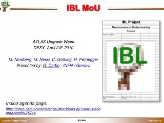
IBL MoU Contribution prepared for Marzio’s talk at April RRB G. Darbo - INFN / Genova
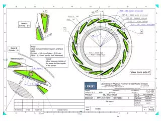
IBL Detector • Material from Raphael/Neal • The present 7m long section of the beam-pipe will be cut (flange too big to pass inside the existing pixel) and extracted in situ: • The new beam-pipe with the IBL will be inserted at its place. PP1 Collar Sealing service ring Alignment wirers Iourii Gusakov IST IBL Support Tube IBL Staves Existing B-layer IBL (Staves)
Technical Status of the Project • FE-I4 – New pixel front-end chip for IBL • 20 x 19 mm2 real-estate, more that 70 M-transistors, largest HEP chip ever. • 2 year design work for a team of ~15 engineers + several physicists from 5 laboratories. • Three design reviews: 17/3/2008, 3-4/11/2009, 16/4/2010 - submission to IBM: 17/5/2010 • Sensor prototypes for FE-I4 under processing – 3 technologies considered: Planar Sensors, 3D Sensors, Diamonds. • Expected sensors bump-bonded to FE-I4 for next fall • IBL Layout finalised – 14 staves with 32 FE-I4 chip modules at R=3.2 cm • Stave baseline (following last December review’s recommendations) • Low density carbon foam (ρ = 0.2 g/cm3), thin wall titanium cooling pipe (d=2mm), CO2 cooling. • Fitting and permanent cooling joints under prototyping. • FEA analysis on going, thermal figure of merit measurement on samples • Mechanical design of the whole IBL detector • 3D model and FEA for the whole detector on going. • Installation mock-up under construction in bld.180 at CERN. • Internal electrical services, flex hybrid in prototype phase. • New ROD/BOC (off-detector readout). • Modernized version of the Pixel VME ROD – more compact (x4 more channels/board) increased performance, large reduction of component count with state of the art FPGA technology.
Memorandum of Understanding • IBL Memorandum of Understanding (MoU) • BetweenThe ATLAS COLLABORATION, andFunding Agency/Institution of the ATLAS Collaboration (for the ATLAS construction was between Institutes and CERN) • IBL MoU – Steps toward project shaping: • “IBL Kick-off” meeting (8/7/2009) – Institutes express their interest in the IBL based on project WBS (Workpackage Breakdown Structure). • Sharing of Resources (draft) discussed in the (interim) Institute Board (1/3/2010) – Contribution to the Cost presented to the National Contact Physicists in ATLAS (ATLAS NCP meeting – 25/2/2010). • IBL interim MoU • Ad Interim MoU until sensor technology is chosen (Planar Silicon / 3D Silicon / Diamond) - Decision on sensor technology (early 2011) – Sensor R&D and IBL communities work in tight collaboration to finalise a design matching IBL specification. • Consolidate interest of Institutes and availability of funds
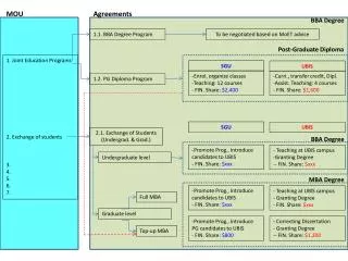
Institutes and Contributions to IBL (Draft) Technology options refer to supplementary costs that are sensor technology specific and will be known before the definite MoU takes effect. So far, France, Italy and US have requested their shares to be moved from M&O to Project part. Note: the numbers in the table "are not final, nor are the suggested financial contributions yet firm, but are meant for a common overall discussion.”
FE-I3 FE-I4 FE-I4 Collaboration: Bonn: D. Arutinov, M. Barbero, T. Hemperek, A. Kruth, M. Karagounis. CPPM: D. Fougeron, M. Menouni. Genova: R. Beccherle, G. Darbo. LBNL: S. Dube, D. Elledge, M. Garcia- Sciveres, D. Gnani, A. Mekkaoui. Nikhef: V. Gromov, R. Kluit, J.D. Schipper The first version of full FE-I4 chip will be submitted by end of March 2010 ~70 million transistors, 0.13 µm CMOS technology 6 Cu and 2 Al routing layers. 20.2mm ~200μm 7.6mm ~19 mm active IBM reticule 16.8mm 8mm active 2.8mm ~2mm Chartered reticule (24 x 32) FE-I3 74% FE-I4 ~89%
IBL Layout • Beam-pipe reduction: • Inner R: 29 25 mm • Very tight clearance: • “Hermetic” to straight tracks in Φ (1.8º overlap) • No overlap in Z: minimize gap between sensor active area. • Layout parameters: • IBL envelope: 9 mm in R • 14 staves. • <R> = 33 mm. • Z = 60 cm (active length). • η = 2.5 coverage.
Annex 4: Tentative Contribution to IBL Technology options refer to supplementary costs that are sensor technology specific and will be known before the definite MoU takes effect. So far, France, Italy and US have requested their shares to be moved from M&O to Project part. Note: the numbers in the table "are not final, nor are the suggested financial contributions yet firm, but are meant for a common overall discussion.”
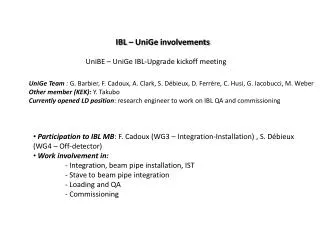
IBL Organisation Structure • Membership • IBL Project Leader: G. Darbo • IBL Technical Coordinator: H. Pernegger • “Module” WG (2 Physicists): F. Hügging & M. Garcia-Sciveres • “Stave” WG (1 Phy. + 1 M.E.): O. Rohne + D. Giugni • “IBL Assembly & Installation” WG (2 M.E. initially, a Phy. Later): N. Hartman + R. Vuillermet • “Off-detector” WG (1 Phy. + 1 E.E.): T. Flick + S. Débieux • “Extra” members: • Ex officio: Upgrade Coordinator (N. Hessey), PO Chair (M. Nessi), Pixel PL (B. Di Girolamo), ID PL (P. Wells), Pixel Chair (C. Gößling) • Offline “liaison” Pixel Off-line coordinator: A. Andreazza • TDR editor (temporary): K. Einsweiler • Whole project divided into 4 working groups • IBL Management Board has 10 members, plus “extra” and ex-officio members. • Frequent meetings (every ~14 days) in this phase of the project. • IBL Management Board • Membership: • IBL PL + IBL TC • 2 coordinators from each WG • Plus “extra” members • Module WG • (2 coordinators) • FE-I4 • Sensors • Bump-Bonding • Modules • Test & QC • Irradiation • Stave WG • (1 Phys + 1 Eng.) • Staves • Cooling Design & Stave Thermal Management • HDI • Internal Services • Loaded Stave • Test & QC • IBL Integr.-Install. • (2 Eng.) • Stave Integration • Global Sup. • Beam Pipe (BP) • Ext.services inst. • IBL+BP Installation • Cooling Plant • Test & QC • Off-detector • (1 Phys + 1 E.Eng.) • Power • DCS • ROD • Opto-link • Ext.serv.design/proc. • Test Beam • System Test