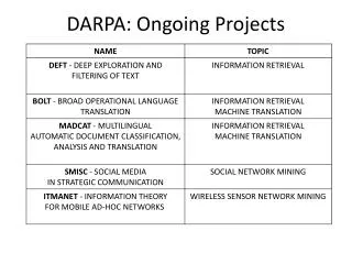
DARPA
DARPA. Digital Audio Receiver, Processor and Amplifier Group Z James Cotton Bobak Nazer Ryan Verret. Uses power transistors in linear region < 50% efficient Performance sensitive to component values Total implementation is bulky. Uses power transistors as switches ~90% efficient

DARPA
E N D
Presentation Transcript
DARPA Digital Audio Receiver, Processor and Amplifier Group Z James Cotton Bobak Nazer Ryan Verret
Uses power transistors in linear region < 50% efficient Performance sensitive to component values Total implementation is bulky Uses power transistors as switches ~90% efficient Component values not an issue One-chip system possible Analog Power Amplifier Digital Power Amplifier
Audio Data Encoding • Pulse Code Modulation (PCM) • Sampled data amplitudes encoded as serial bit stream • Standard method of encoding • Pulse Width Modulation (PWM) • Sampled data amplitudes encoded as pulse duty cycle • Can directly drive power transistors LPF PCM PWM
Real World Interface • S/PDIF • consumer transmission standard • too complex to decode on chip • Solution: • TI DIR1703 • S/PDIF to PCM converter • Result: • Our chip should run off the digital output from a DVD player as well as drive speakers. DIR1703 with Evaluation Board
Algorithm Overview • Shift in PCM data, truncate to 12 bit words • Upsample to 2*fs • Decreases artifacts in final output • Uses a 14-tap IIR filter with loadable 8-bit coefficients • Load upsampled data to fast 8-bit counter • Toggle PWM output using counter overflow and load
Block Diagram 32 8 8 8 8 PCM Stream Serial Shift In FIR Coefficients FIR Coefficients IIR Coefficients IIR Coefficients New Data 7 7 12 Overflow Detector 12 12 + 12 PWM Out 12 + 9 + 12 12 + Counter Past Values Past Values 7 12 12 12 + 12
System Control • System operations run on a 256*fs, two-phase clock • 128 clock cycles available per interpolation • System goes through states in a set pattern • PLA unnecessary • 8-bit counter that is decoded with a customized control decoder
Input Stage • Serially shifts in audio data • IIS Bus Specification • L/R channel select • Drops top 12 bits into a FIFO • Holds 7 data words • Addressable data bus • Results in 7 available past values for FIR filtering
Basic Adder Cell • Two’s complement one bit adder cell • Optimized for horizontal data routing and vertical control routing • Dimensions optimized for vertical stacking • No use of metal2 or metal3
Multiply and Accumulate Block • 12-by-8 to 12 bit multiplier • Signed multiplication by using add-shift-accumulate with sign extension • Adder shares accumulator with multiplier • Accumulator from multiplier sums seven multiplies • Multiply-and-accumulate makes for efficient IIR filtering
8-bit Counter • Increments 256 times per interpolated sample • Must run on a 512*fs, single-phase clock • Synchronous counter used to reduce propagation delay • PWM output goes high on overflow, low on sample load • Resolution doubling • allowing PWM output to change on either rising or falling edge based on 9th bit
Timing Analysis • Chip must run in sync with TI DIR1703 • Several large blocks must run at very high speeds to keep up • Crystal timing of longest path • Ex: Adder longest path ~6ns • Extensive spice simulation of large blocks • Ex: Counter spice run
Status • Large blocks completed and tested in IRSIM and SPICE • Full layout and datapath routing complete • Remaining: • Simulation from padframe on full layout • Power and ground routing (metal3 reserved for this purpose) • Minor control routing
Testing Strategy • Shift in data and coefficients serially • Verify data integrity • Check addition and multiplication accuracy • Ensure PWM output transitions properly • Testing bus used to look at internal data off-chip • Bypass processing mode • Test vectors extremely large even for short time duration • Cannot simulate length audio data conversion in IRSIM • Solution: Matlab
Simulation • Algorithm fully simulated in Matlab • Data truncation and quantization accounted for • Next semester: Real-time audio processing and amplification
Simulation Result • Success! • Audio quality well-preserved through processing