Download
1 / 8
80 likes | 107 Views
In this work the effect of laser pulse energy on the optical properties of five samples of SiO2 thin film deposited using pulse laser deposition technique was studied. Pulse energies of 100,150,180, 200 and 250 mj with fixed pulse repetition rate and number of pulses of 2 Hz, and 10 pulses, were used. The target to substrate distance and angle were fixed. The film thickness was measured by FESEM, and the transmission spectrum at certain wavelengths for each film was recorded. SiO2 thin films transmission data and the measured film thicknesses were used to deduce their optical properties. The results showed that increasing the pulse energy results in an increase of the film thickness and the morphology of the films becomes more dense and non smooth at higher pulse energy, also the optical properties showed to be affected by the thickness variation and hence by the pulse energy. Nafie A. Almuslet | Yousif H. Alsheikh | Kh. M. Haroun "Pulse Energy Effect on the Optical Properties of Pulse Laser Deposited SiO2 Thin Films" Published in International Journal of Trend in Scientific Research and Development (ijtsrd), ISSN: 2456-6470, Volume-2 | Issue-6 , October 2018, URL: https://www.ijtsrd.com/papers/ijtsrd18341.pdf Paper URL: http://www.ijtsrd.com/mathemetics/-/18341/pulse-energy-effect-on-the-optical-properties-of-pulse-laser-deposited-sio2-thin-films/nafie-a--almuslet<br>

E N D
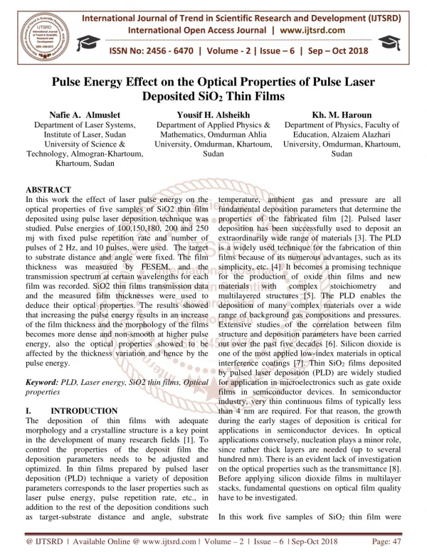
International Journal of Trend in Scientific Research and Development (IJTSRD) International Open Access Journal | www.ijtsrd.com ISSN No: 2456 - 6470 | Volume - 2 | Issue – 6 | Sep – Oct 2018 Pulse Energy Effect on the Optical Properties of Pulse Laser Deposited SiO2 Thin Films Nafie A. Almuslet Department of Laser Systems, Institute of Laser, Sudan University of Science & Technology, Almogran-Khartoum, Khartoum, Sudan ABSTRACT In this work the effect of laser pulse energy on the optical properties of five samples of SiO2 thin film deposited using pulse laser deposition technique was studied. Pulse energies of 100,150,180, 200 and 250 mj with fixed pulse repetition rate and number of pulses of 2 Hz, and 10 pulses, were used. The target to substrate distance and angle were fixed. The film thickness was measured by FESEM, and the transmission spectrum at certain wavelengths for each film was recorded. SiO2 thin films transmission data and the measured film thicknesses were used to deduce their optical properties. The results showed that increasing the pulse energy results in an increase of the film thickness and the morphology of the films becomes more dense and non-smooth at higher pulse energy, also the optical properties showed to be affected by the thickness variation and hence by the pulse energy. Keyword: PLD, Laser energy, SiO2 thin films, Optical properties I. INTRODUCTION The deposition of thin films with adequate morphology and a crystalline structure is a key point in the development of many research fields [1]. To control the properties of the deposit film the deposition parameters needs to be adjusted and optimized. In thin films prepared by pulsed laser deposition (PLD) technique a variety of deposition parameters corresponds to the laser properties such as laser pulse energy, pulse repetition rate, etc., in addition to the rest of the deposition conditions such as target-substrate distance and angle, substrate Yousif H. Alsheikh Department of Applied Physics & Mathematics, Omdurman Ahlia University, Omdurman, Khartoum, Sudan Kh. M. Haroun Department of Physics, Faculty of Education, Alzaiem Alazhari University, Omdurman,Khartoum, Sudan temperature, ambient gas and pressure are all fundamental deposition parameters that determine the properties of the fabricated film [2]. Pulsed laser deposition has been successfully used to deposit an extraordinarily wide range of materials [3]. The PLD is a widely used technique for the fabrication of thin films because of its numerous advantages, such as its simplicity, etc. [4]. It becomes a promising technique for the production of oxide thin films and new materials with complex multilayered structures [5]. The PLD enables the deposition of many complex materials over a wide range of background gas compositions and pressures. Extensive studies of the correlation between film structure and deposition parameters have been carried out over the past five decades [6]. Silicon dioxide is one of the most applied low-index materials in optical interference coatings [7]. Thin SiO2 films deposited by pulsed laser deposition (PLD) are widely studied for application in microelectronics such as gate oxide films in semiconductor devices. In semiconductor industry, very thin continuous films of typically less than 4 nm are required. For that reason, the growth during the early stages of deposition is critical for applications in semiconductor devices. In optical applications conversely, nucleation plays a minor role, since rather thick layers are needed (up to several hundred nm). There is an evident lack of investigation on the optical properties such as the transmittance [8]. Before applying silicon dioxide films in multilayer stacks, fundamental questions on optical film quality have to be investigated. In this work five samples of SiO2 thin film were stoichiometry and @ IJTSRD | Available Online @ www.ijtsrd.com | Volume – 2 | Issue – 6 | Sep-Oct 2018 Page: 47
International Journal of Trend in Scientific Research and Development (IJTSRD) ISSN: 2456-6470 fabricated using pulsed laser deposition using Q- switched Nd:YAG with the wavelength of 1064 nm, 10 pulses with pulse repetition rate of 2 Hz, the target to substrate distance and angle were fixed to 2 cm and 45o , respectively. Varied pulse energy of 100,150, 180, 200 and 250 mj were used. The film thickness was measured by Field Emission scanning Electron Microscope (FESEM) measurement tool, and the transmission spectrum at certain wavelengths for each film was recoded. SiO2 thin films transmission data and the measured film thicknesses were used to calculate their optical properties. II. MATERIALS, TOOLS AND METHODS: A. MATERIALS: The material used in this work were silicon dioxide (SiO2) of 99.9% purity and refractive index of 1.46 it was prepared in disc form by mixing 50:50 ratio of the SiO2 powder and Potassium bromide (IR spectroscopy grade). B. TOOLS AND EQUIPMENTS: Different tools and equipments were used to complete this work. They are described below with their specifications and needs: 1.Pressing machine: A hand press machine manufactured by Shimadzu (Japan) was used in this work [10]. The machine is used to press the SiO2 powder in disc form (after mixing with Potassium Bromide) for target ablation. 2.Q- Switched Nd: YAG Laser: Q-switched Nd: YAG model OW D1 [11] was used to deposit SiO2 thin film. 3. Scanning Electron Microscope (FESEM): Scanning electron microscopy type TESCAN MIRA 3 was used to measure the films thickness. MIRA3 is a high performance SEM system which gives high resolution and low-noise imaging [12]. MIRA3 offers all the advantages that come with the latest technologies and developments in SEM; delivering faster image acquisition, an ultra-fast scanning system, dynamic compensation and built-in scripting for user- defined applications [13]. 4.DIFFERENT LIGHT SOURCES: Different monochromatic light sources were used to record the transmission spectra for the fabricated films [13-15]. Table 1: the monochromatic light sources used in this work and static Wavelength (nm) 532 632.8 660 675 Light Source Diode Laser He-Ne Laser Diode laser Omega XP Laser (red probe) Omega XP Laser (IR 820 nm probe) Omega XP Laser (IR 915 nm probe) 820 915 5.THE PHOTODETECTOR: A silicon pin photodiode was used in this work for detecting the transmitted intensity of each light source after passed through the fabricated SiO2 films. C. THE METHOD: The procedure to fabricate SiO2 thin films and study the effect of the pulse energy on their properties was done as follows: ➢The experimental setup used to produce SiO2 thin films was arranged as shown in figure (1). ➢Different disks of SiO2 (as targets) were prepared by the press machine. Figure 1: Schematic diagram of the experimental setup for fabrication of SiO2 thin films @ IJTSRD | Available Online @ www.ijtsrd.com | Volume – 2 | Issue – 6 | Sep-Oct 2018 Page: 48
International Journal of Trend in Scientific Research and Development (IJTSRD) ISSN: 2456-6470 ➢The distance and the angle between the target and the glass substrate were fixed to 2 cm, and 45o, respectively. ➢The glass substrates were cut into the dimensions suitable for SEM imaging 2X2 cm, and then washed with distilled water and cleaned with alcohol. ➢The Q-Switched Nd: YAG laser machine was switched on and 10 pulses with energy of 100 mj and a R.R. of 2 Hz was used to deposit SiO2 thin film on the glass substrate. ➢The above step was repeated four times with varied pulse energy of 150, 180, 200 and 250 mj with fixed repetition rate and number of pulses. ➢The fabricated SiO2 thin films were examined using FESEM to measure their thicknesses. ➢The relation between the laser pulse energy and the SiO2 thin film thickness was plotted. ➢The transmission spectra of the fabricated SiO2 films were recorded monochromatic light sources. ➢Thicknesses of the SiO2 films and the transmission data were used to calculate the optical properties for each film. ➢The refractive index of each thin film was calculated using the measured reflectivity R and the glass refractive index μs according to:[16, 17]. 1 ) 1 − R (1) where Ts represents the transmission of the glass substrate. ➢The absorption coefficients were deduced from the measured value of reflectivity R, the transmittance T, refractive index μs, and thickness t according to [16,17]: R t III. RESULTS AND DISCUSSION: The results presented here were composed of two parts: a- the influence of the pulse energy deposition parameter of the PLD on the thickness of the fabricated SiO2 thin films and b- the effect of the pulse energy on the optical properties of the produced SiO2 thin films. A.Pulse energy effect on the thickness of the SiO2 thin films: The five samples of the SiO2 thin films using 10 pulses with pulse repetition rate of 2 Hz and varying pulse energies of 100, 150, 180, 200 and 250 mj. Then the five deposited SiO2 thin film samples were imaged using FESEM machine and their thicknesses were measured and tabulated in table (2) with the corresponding pulse energy used. Figure (2-1a) shows the morphology of the SiO2 thin films deposited using laser pulse energy of 100 mj and figure (2-1b) shows the FESEM thickness measurement of the produced SiO2 thin film. − 2) 1 1 ( (2) = T using different + 1 [ s ] R = ( 2 1 1 T 1 = − ( 1 ) 2 s 2 T s s Figure 2-1 a: SiO2 thin film deposited on glass substrate with laser energy of 100 mj and repetition rate of 2 Hz @ IJTSRD | Available Online @ www.ijtsrd.com | Volume – 2 | Issue – 6 | Sep-Oct 2018 Page: 49
International Journal of Trend in Scientific Research and Development (IJTSRD) ISSN: 2456-6470 Figure 2-1 b: The thickness measurement of the SiO2 thin film deposited on glass substrate with laser energy of 100 mj and repetition rate of 2 Hz The FESEM image together with the thickness measurement shown in figures (2-1a, and b), respectively, illustrate that the SiO2 thin film has a thickness of 0.39 µm and it's clear that the fabricated film is dense and has smooth film morphology. Figure 2-2 a: SiO2 thin film deposited on glass substrate with laser energy of 250 mj and repetition rate of 2 Hz Figure (2-2 a) shows the SiO2 thin film that was achieved laser pulse energy of 250 mj, while the number of pulses, the pulse repetition rate and other deposition parameters were the same. The film thickness that results when the pulse energy was 250 mj is shown in figure (2-2 b). Figure 2-2 b: The thickness measurement of SiO2 thin film deposited on glass substrate with laser energy of 250 mj and repetition rate of 2 Hz Also figure (2-2 a) proved this film is dense and with non-smooth morphology compared to the first film in figure (2-1 a) and this is due to the increasing the pulse energy. @ IJTSRD | Available Online @ www.ijtsrd.com | Volume – 2 | Issue – 6 | Sep-Oct 2018 Page: 50
International Journal of Trend in Scientific Research and Development (IJTSRD) ISSN: 2456-6470 Table 2: thicknesses of the five fabricated SiO2 thin films versus laser pulse energy: Pulse energy in (mj) with R.R = 2 Hz Samples codes SiO2 thin film thickness in (µm) 100 150 180 200 250 S1 S2 S3 S4 S5 0.39 0.52 0.58 0.62 0.71 The relation between the SiO2 thin film thickness and the pulse energy is plotted in figure 3 and the equation that best describe the deposited thin film thickness energy relation was obtained. Thickness of SiO2thin film vs Pulse energy Y-axis represent the Thickness of the SiO2 thin film, 1 cm =0.05 µm X-axis represent the Pulse energy used for the deposition, 1 cm = 20 mj Best fitting of the results gives: Thickness of SiO2 thin films = A+B1EP+B2E2 A=0.08492, B1= 0.00344, and B2=-3.77267E-6 0.75 P 0.70 0.65 0.60 Thickness / µm 0.55 0.50 0.45 0.40 0.35 100 120 140 160 Pulse energy/ mj 180 200 220 240 260 Figure 3: The SiO2 thin film thicknesses versus laser pulse energy used for the deposition From figure 3 it was found that the thickness of the deposited SiO2 thin films is dependent on the pulse energy used and the equation relate the film thickness and the laser pulse energy is: AE Thickness P = Where EP is the energy of the pulse while A, B1 and B2 being constants and their values were shown in figure (3). Also it is clear that increasing the pulse energy results in an increment of the film thickness. B.THE OPTICAL PROPERTIES OF THE FABRICATED SIO2 FILMS: Optical measurement constitutes the most important means of determining the band structure of the materials [18]. Optical constants of thin films provide us with information characteristics of the material and its determination is very important for using it in any of such devices [19]. The transmission spectra, refractive indices and absorption coefficients were obtained for each SiO2 thin film. The transmission intensities of different monochromatic light sources were detected before and after deposition for the five SiO2 thin films and the results of sample S1 are tabulated in table (3): concerning microscopic + + 2 (3) BE C P Table 3: Intensities before and after the deposition of sample S1 (of thickness =0.39 µm): Wavelength (nm) Io± 0.001 (V) 532 340 632.8 401 660 442 675 472 820 526 915 385 Intensity before deposition Intensity after deposition I ± 0.001 (V) 319 361 404 436 490 343 @ IJTSRD | Available Online @ www.ijtsrd.com | Volume – 2 | Issue – 6 | Sep-Oct 2018 Page: 51
International Journal of Trend in Scientific Research and Development (IJTSRD) ISSN: 2456-6470 The data in table (3) above was used to calculate the T% (T = I/I0) at the given wavelengths for sample S1 and the same was done with the other four samples. The calculated values are plotted for the fives samples S1, S2, S3, S4 and S5 in figure (4) as a function of wavelength. Transmission % vswavelengths for five samples SiO2 thin films Y-axis represent the transmission %, 1 cm =0.02 % X-axis represent the wavelengths, 1 cm =50 nm Transmission f SiO2 thin film sample S5 Transmission f SiO2 thin film sample S4 Transmission f SiO2 thin film sample S3 Transmission f SiO2 thin film sample S2 Transmission f SiO2 thin film sample S1 0.98 0.97 0.96 0.95 0.94 Transmission % 0.93 0.92 0.91 0.90 0.89 0.88 500 550 600 650 700 750 800 850 900 950 Wavelength/ nm Figure 4: transmission spectra of the five SiO2 thin film samples Figure 4 show that the thickness of the thin film affected its transmission, the large thickness of the thin film a gives the lower transmission of the film. Regarding the thickness difference shown in figure 4, it can be said that the SiO2 thin films have a high transparency varied from (0.89-0.97) % in the investigated spectral range. The calculated refractive indices for the five samples using equation (1) are plotted as a function of wavelengths as shown in figure (5). Refractive indices of SiO2 thin films vs wavelengths Y-axis represent the refractive indices, 1 cm =0.02 X-axis represent the wavelengths, 1 c =50 nm Refractive indices of SiO2 thin film sample S5 Refractive indices of SiO2 thin film sample S4 Refractive indices of SiO2 thin film sample S3 Refractive indices of SiO2 thin film sample S2 Refractive indices of SiO2 thin film sample S1 1.80 1.74 1.68 Refractiveindices 1.62 1.56 1.50 1.44 1.38 500 550 600 650 700 750 800 850 900 950 Wavelengths/nm Figure 5: The refractive index of the five samples of SiO2 thin films versus wavelengths @ IJTSRD | Available Online @ www.ijtsrd.com | Volume – 2 | Issue – 6 | Sep-Oct 2018 Page: 52
International Journal of Trend in Scientific Research and Development (IJTSRD) ISSN: 2456-6470 Figure 5 shows that sample S1 which is of smallest thickness among the other has highest refractive indices from 532 to 660 nm. The refractive index of any material in thin film profile is usually deviates from that of the bulk of the same material. This is due to the void fraction typical of the thin film microstructure [20]. The absorption coefficients calculated for the deposited SiO2 film samples using equation (2) are plotted versus wavelengths in figure (6). Absorption coefficients of five samples of SiO2 thin films vs wavelengths Y-axis represent the absorption coefficients, 1 cm = 2*103 cm-1 X-axis represent the wavelengths, 1 cm = 50 nm Absorption coefficientsof SiO2 thin film sample S1 Absorption coefficients of SiO2 thin film sample S2 Absorption coefficients of SiO2 thin film sample S3 Absorption coefficients of SiO2 thin film sample S4 Refractive indices of SiO2 thin film sample S5 50 48 46 44 42 -1 40 Absorption coefficients/ cm 38 36 34 32 30 28 26 24 22 20 18 500 550 600 650 700 750 800 850 900 950 Wavelengths/ nm Figure 6: Absorption coefficients versus wavelengths for five samples of SiO2 Figures (5) and (6) support the idea of using such film as an optical filter or as a reflector in specific wavelengths deduced from the transmission spectrum. The refractive indices and absorption coefficients of the pulsed laser deposited SiO2 thin films varies with thickness and for each thickness the transmission is unique, therefore these two optical properties are functions of the film thickness and therefore depend on the pulse energy used for the deposition of such films. IV. CONCLUSION: From the obtained results the followings can be concluded: ➢SiO2 thin films of different thicknesses and optical properties can be produced using pulsed laser deposition technique. ➢Pulse energy of the laser source is an important parameter in fabrication of films prepared using PLD method. ➢The thickness of the SiO2 thin film can be controlled by controlling the pulse energy used in the deposition process. ➢The SiO2 can be used to produce optical components in the range from 532 nm to 915 nm by controlling its thickness. REFERENCES: 1.Antonella Lorusso et al., Characterisation of Pb thin films prepared by the nanosecond pulsed laser deposition technique for photocathode application, 2015, Thin Solid Films, (579) , 50-56 2.Hashmi, J Z, Siraj, K, Latif, A et al., Study of deposition parameters for the fabrication of ZnO thin films using femto second laser. (2016) Applied Physics A: Materials Science and Processing, 122 (8). ISSN 0947-8396 3.M. C. RAO, PULSED LASER DEPOSITION — ABLATION MECHANISM APPLICATIONS, International Modern Physics: Conference Series, Vol. 22 (2013) 355–360 4.J. Shen, Zheng Gai, and J. Kirschner, Growth and magnetism of metallic thin films and multilayers by pulsed-laser deposition, Surface Science Reports 52 (2004) 163–218 5.Đekić M et al., Influence of deposition parameters on pulsed laser deposition of K0.3MoO3 thin films, Bulletin of the Chemists and Technologists of Bosnia and Herzegovina, volume 48, (2017) pp.1-4. AND Journal of @ IJTSRD | Available Online @ www.ijtsrd.com | Volume – 2 | Issue – 6 | Sep-Oct 2018 Page: 53
International Journal of Trend in Scientific Research and Development (IJTSRD) ISSN: 2456-6470 6.PVD Products, PLD overview, Pulse-Laser deposition system available http//www.pvdproducts.com/pulsed-laser- deposition-systems/pld-overview, visited 5/June 2018 7.Oili Ylivaara et al., Residual stress in SiO2 thin films on silicon,(2016) In Stress Evolution in Thin Films and Coatings Book of Abstracts [17] American Vacuum Society AVS. 8.Kristin Pfeiffer et al.,Comparative study of ALD SiO2 thin films for optical applications, OPTICAL MATERIALS EXPRESS (2016) 660, Vol. 6, No. 2 9.Shimadzu hand press information (P/N Corporation, Japan 2013 10.Q-Switched Nd:YAG, Beijing Oriental Wison Technology Co., LimitedModel no OW D1, product information, 2017 11.Arun Singh Chouhan, Tuning of Magnetic and Electrical Properties in Complex oxide Thin Films Deposited By Pulsed Laser Deposition, M.Sc thesis, Indian Institute of Technology Patna, India, 2015 12.Microscopy - MATERIAL SCIENCE - Electron Microscopy – Tescan, MIRA3, [online] available from https://www.wirsam.com/product/mira-3, visited, 16/2/2018 13.Phywe, Helium Neon Laser Products 8181-93 Info. https://www.phywe.de/en/geraetehierarchie/physic s/modern-physics/quantum-physics/08181-93 14.Oriental Wison, ,1320/1064/532 nm Q-switched Nd: YAG laser, Model Name OW-D, product datasheet, Beijing Oriental Wison Mechanical & Electronic Co., Ltd, 2017, China. 15.Biotechhealth, Omega XP laser system and product datasheet, http//www.biotechhealth.co.uk. 16.Nafie A. Almuslet and Yousif H. Alsheikh, Investigation of the Optical Properties of Liquid Deposition CuSO4 Thin Film, IJSRST, Volume 1, issue 5, pp. 132-136, December, 2015. 17.A. M. Mousa and J. P. Ponpon, Growth of Pb Te films by laser induced evaporation of pressed Pb Te pellets, Eur. Phys. J. Appl. Phys., 2006 18.M. T. Hussein, E. M. Nasir, and A. H. Al-Aarajiy, Study on the UV-Visible of Ni-Phthalocyanine thin film Optical Properties, Int. J. Thin Film Sci. Tec. 1, (2012) No. 2, 71-76 19.Geunther Karl H., Physical and Chemical Aspects in the Application of Thin Film on Optical Element, Optical Society of America, 1984 [online] from 2007, machine, product Shimadzu 2011 200-64174), @ IJTSRD | Available Online @ www.ijtsrd.com | Volume – 2 | Issue – 6 | Sep-Oct 2018 Page: 54