Digital Logic Design Basics
60 likes | 81 Views
The digital logic design is a system in electrical and computer engineering that uses simple numerical values to produce input and output operations. As a digital design engineer, you may assist in developing cell phones, computers, and related personal electronic devices. In the modern world of electronics, the term digital is usually associated with a computer. This is due to the fact that the term digital is derived from the way the computers perform operations, by counting digits. Nowadays digital concepts are usually applied to various problems which are solved by analog methods. In modern times digital systems find applications related to industrial and consumer products which maintain and develop various ways which develop our country and helps in developing science ideas in terms of research. As computer science is upgraded in every way it helps to develop the multinational companies in the form of bonus machines. Durgesh Raghuvanshi "Digital Logic Design: Basics" Published in International Journal of Trend in Scientific Research and Development (ijtsrd), ISSN: 2456-6470, Volume-3 | Issue-1 , December 2018, URL: https://www.ijtsrd.com/papers/ijtsrd18948.pdf Paper URL: http://www.ijtsrd.com/computer-science/other/18948/digital-logic-design-basics/durgesh-raghuvanshi<br>

Digital Logic Design Basics
E N D
Presentation Transcript
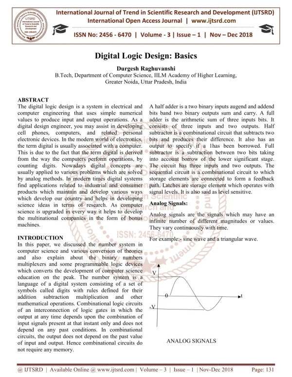
International Journal of Trend in International Open Access Journal International Open Access Journal | www.ijtsrd.com International Journal of Trend in Scientific Research and Development (IJTSRD) Research and Development (IJTSRD) www.ijtsrd.com ISSN No: 2456 ISSN No: 2456 - 6470 | Volume - 3 | Issue – 1 | Nov 1 | Nov – Dec 2018 Digital Logic Digital Logic Design: Basics Durgesh Raghuvanshi B.Tech, Department of Computer Science, IILM Academy of Higher Learning, Greater Noida, Uttar Pradesh, India Greater Noida, Uttar Pradesh, India ech, Department of Computer Science, IILM Academy of Higher Learning, ech, Department of Computer Science, IILM Academy of Higher Learning, ABSTRACT The digital logic design is a system in electrical and computer engineering that uses simple numerical values to produce input and output operations. As a digital design engineer, you may assist in developing cell phones, computers, and related personal electronic devices. In the modern world of electronics, the term digital is usually associated with a computer. This is due to the fact that the term digital is derived from the way the computers perform operations, by counting digits. Nowadays digital conce usually applied to various problems which are solved by analog methods. In modern times digital systems find applications related to industrial and consumer products which maintain and develop various ways which develop our country and helps in dev science ideas in terms of research. As computer science is upgraded in every way it helps to develop the multinational companies in the form of bonus machines. INTRODUCTION In this paper, we discussed the number system in computer science and various conversion of theories and also explain about the binary numbers multiplexers and some programmable logic devices which converts the development of computer science education on the peak. The number language of a digital system consisting of a set of symbols called digits with rules defined for their addition subtraction multiplication mathematical operations. Combinational logic circuits of an interconnection of logic gates in which the output at any time depends upon the combination of input signals present at that instant only and does not depend on any past conditions. In combinational circuits, the output does not depend on the past value of input and output. Hence combinational circuits do not require any memory. A half adder is a two binary inputs augend and addend bits band two binary outputs sum and carry. adder is the arithmetic sum of three inputs bits. It consists of three inputs and two outputs. Half subtractor is a combinational circuit that subtracts two bits and produces their difference. It also has an output to specify if a 1has been borrowed. Full subtractor is a subtraction between two bits taking into account borrow of the lower significant stage. The circuit has three inputs and two outputs. sequential circuit is a combinational circuit to which storage elements are connected to form a feedback path. Latches are storage element which operates with signal levels. It is also said as level sensitive. also said as level sensitive. The digital logic design is a system in electrical and computer engineering that uses simple numerical values to produce input and output operations. As a digital design engineer, you may assist in developing cell phones, computers, and related personal ectronic devices. In the modern world of electronics, the term digital is usually associated with a computer. This is due to the fact that the term digital is derived from the way the computers perform operations, by counting digits. Nowadays digital concepts are usually applied to various problems which are solved by analog methods. In modern times digital systems find applications related to industrial and consumer products which maintain and develop various ways which develop our country and helps in developing science ideas in terms of research. As computer science is upgraded in every way it helps to develop the multinational companies in the form of bonus adder is a two binary inputs augend and addend bits band two binary outputs sum and carry. A full sum of three inputs bits. It and two outputs. Half subtractor is a combinational circuit that subtracts two bits and produces their difference. It also has an output to specify if a 1has been borrowed. Full subtractor is a subtraction between two bits taking e lower significant stage. The circuit has three inputs and two outputs. The sequential circuit is a combinational circuit to which storage elements are connected to form a feedback path. Latches are storage element which operates with Analog Signals: Analog signals are the signals which may have an er of different magnitudes or values. Analog signals are the signals which may have an infinite number of different magnitudes or values. They vary continuously with time. They vary continuously with time. For example:- sine wave and a triangular wave sine wave and a triangular wave. discussed the number system in computer science and various conversion of theories and also explain about the binary numbers multiplexers and some programmable logic devices which converts the development of computer science V umber system is a system consisting of a set of symbols called digits with rules defined for their addition subtraction multiplication mathematical operations. Combinational logic circuits of logic gates in which the output at any time depends upon the combination of input signals present at that instant only and does not depend on any past conditions. In combinational the output does not depend on the past value input and output. Hence combinational circuits do 0 t and and other other -V ANALOG SIGNALS @ IJTSRD | Available Online @ www.ijtsrd.com www.ijtsrd.com | Volume – 3 | Issue – 1 | Nov-Dec 2018 Dec 2018 Page: 131
International Journal of Trend in Scientific Research and Development (IJTSRD) ISSN: 2456 International Journal of Trend in Scientific Research and Development (IJTSRD) ISSN: 2456 International Journal of Trend in Scientific Research and Development (IJTSRD) ISSN: 2456-6470 Digital Signals: Drawbacks:- 1.Analysis of an analog system is less accurate. 2.Analysis of analog system requires time domain analysis which requires a very sound mathematical background. 3.Analog systems are usually affected more by the undesired electrical disturbance called noise. 4.The performance of analog systems degrades because of component 5.Their performance changes due to variation in temperature. Analysis of an analog system is less accurate. analog system requires time- domain analysis which requires a very sound mathematical background. Analog systems are usually affected more by the undesired electrical disturbance called Parameter comparison No. of values Nature signals Sources signals of Analog signals Digital signals Digital signals Infinite Continuous time Discrete Finite Finite Discrete-time of of Signal generators, transducers etc. Sine wave, a triangular wave Computers, A to D converters etc. Binary signal Binary signal Computers, A to D converters etc. The performance of analog systems degrades because of component aging. Their performance changes due to variation in Examples A signal is known as a digital signal if it has only a finite number of predetermined distinct magnitudes. Depending upon the number of distinct magnitudes, the digital signals may be classified as under: the digital signals may be classified as under: A signal is known as a digital signal if it has only a Floating point representation:- - tinct magnitudes. Integers are whole numbers or fixed point numbers with the radix point fixed after the least significant bit. They are contrasted to real numbers or floating numbers where the position of the radix point varies. They are posts on a representation of floating point format. The objective of this is to provide the number of bits is finalized for a particular system we cannot change it abruptly. Hence for ab we can represent is (0)2 which is to increase the range of the numbers to be represented an obvious solution is to increase the number of bits. is to increase the number of bits. Integers are whole numbers or fixed point numbers with the radix point fixed after the least significant bit. They are contrasted to real numbers or floating point numbers where the position of the radix point varies. They are posts on a representation of floating point format. The objective of this is to provide the number of bits is finalized for a particular system we cannot change it abruptly. Hence for above format number, we can represent is (0)2 which is to increase the range of the numbers to be represented an obvious solution Depending upon the number of distinct magnitudes, Actually, the digital signals are discrete time signals that are they are not continuous. the digital signals are discrete time signals 1 Binary codes:- The digital data is represented stored and transmitted its. The group of bits also binary code. They are classified as numeric and alphanumeric codes are used to represent a The digital data is represented stored and transmitted as groups of binary digits. The group of bits also known as binary code. They are classified as numeric and alphanumeric codes are used to represent a character. Serial no. No. of distinct magnitudes 2 8 16 Types of digital signals Binary Octal Hexadecimal Hexadecimal Types of digital signals Binary Octal 1 2 3 Classification of binary codes: Classification of binary codes:- Weighted codes:- Comparison of digital and analog signals: of digital and analog signals: In weighted codes, each digit is assigned a specific weight according to its position. For example, in 8421BCD code, 1001 the weights of 1, 0, 0, 1 (from left to right) are 8, 4, 2 and 1 respectively. left to right) are 8, 4, 2 and 1 respectively. In weighted codes, each digit is assigned a specific weight according to its position. For example, in 8421BCD code, 1001 the weights of 1, 0, 0, 1 (from Analog systems: The system which process the analog signals are called as analog systems. The system which process the analog signals are Suppose W1' W2' W3 and W4 are the weights of igits and Xl' X2, X3 and X4 are the corresponding digit values then decimal digit. N = W1 Xl + W2 X2 + W3 X3 + W4 X4 is represented by Suppose W1' W2' W3 and W4 are the weights of binary digits and Xl' X2, X3 and X4 are the corresponding digit values then decimal digit. N = W1 Xl + W2 X2 + W3 X3 + W4 X4 is represented by binary sequence X4 X3 X2 X4. binary sequence X4 X3 X2 X4. Examples:- 1.Filters circuit 2.Amplifier circuits 3.Signal generators 4.Motor speed controllers The codes 8421BCD, 2421BCD, 5211BCD are all The codes 8421BCD, 2421BCD, 5211BCD are all weighted codes. @ IJTSRD | Available Online @ www.ijtsrd.com www.ijtsrd.com | Volume – 3 | Issue – 1 | Nov-Dec 2018 Dec 2018 Page: 132
International Journal of Trend in Scientific Research and Development (IJTSRD) ISSN: 2456 International Journal of Trend in Scientific Research and Development (IJTSRD) ISSN: 2456 International Journal of Trend in Scientific Research and Development (IJTSRD) ISSN: 2456-6470 Quine–McCluskey algorithm, later followed by the Espresso heuristic logic minimizer, the rapidly improving chip densities, and the wide adoption of HDLs for circuit description, formalized the logic optimization domain as it exists today. optimization domain as it exists today. McCluskey algorithm, later followed by the o heuristic logic minimizer, the rapidly improving chip densities, and the wide adoption of HDLs for circuit description, formalized the logic Non-weighted codes:- The non-weighted codes are not positionally weighted. In other words, each digit position within the number is not assigned a fixed value ( or weight ). the number is not assigned a fixed value ( or weight ). weighted codes are not positionally weighted. In other words, each digit position within Excess-3 and gray code are non-weighted codes. weighted codes. Today, logic optimization is divided into various Today, logic optimization is divided into various categories: Alphanumeric codes:- i. ii. iii. iv. v. vi. vii. viii. ix. x. Based on the circuit representation Two-level logic optimization Multi-level logic optimization Based on circuit characteristics Sequential logic optimization Combinational logic optimization Based on the type of execution Graphical optimization methods Tabular optimization methods Algebraic optimization methods Algebraic optimization methods on the circuit representation level logic optimization level logic optimization Based on circuit characteristics Sequential logic optimization Combinational logic optimization Based on the type of execution Graphical optimization methods Tabular optimization methods Codes used to represent numbers, alphabetic characters, symbols and various instructions necessary for conveying intelligible information. numbers, alphabetic characters, symbols and various instructions necessary ASCII, EBCDIC, UNICODE are the most used alphanumeric codes. ASCII, EBCDIC, UNICODE are the most-commonly Error detecting and correcting codes:- Codes which allow error detection and correction are called error detecting and' correcting codes. Hamming code is the most commonly used error detecting and correcting code. w error detection and correction are called error detecting and' correcting codes. Hamming code is the most commonly used error detecting and level circuit representation of circuits strictly refers to the flattened view of the circuit in products) — which is more applicable to a PLA implementation of the design[clarification needed] representation is a more generic view of the circuit in terms of arbitrarily connected SOPs, POSs (product- sums), factored form etc. Logic optimization algorithms generally work either on the structural (SOPs, factored form) or functional (BDDs, ADDs) While a two-level circuit representation of circuits strictly refers to the flattened view of the circuit in terms of SOPs (sum-of-products) applicable to a PLA implementation of design[clarification needed] representation is a more generic view of the circuit in terms of arbitrarily connected SOPs, POSs (product of-sums), factored form etc. Logic optimization algorithms generally work either on the structural (SOPs, factored form) or functional (BDDs, ADDs) representation of the circuit. Reflective codes:- — a multi-level A code is reflective when the code is self complementing. In other words, when the code for 9 is the complement the code for 0, 8 for 1, 7 for 2, 6 for 3 and 5 for 4. A code is reflective when the code is self- en the code for 9 is the complement the code for 0, 8 for 1, 7 for 2, 6 2421BCD, 5421BCD and Excess-3 code are reflective codes. 3 code are reflective Duality principle:- Sequential codes:- It states that in a two-valued Boolean of an algebraic expression can be obtained simply by interchanging OR and AND operators and by replacing IS by OS and OS by IS. placing IS by OS and OS by IS. valued Boolean algebra the dual In sequential codes, each succeeding 'code is one binary number greater than its preceding code. This property helps in the manipulation of data. property helps in the manipulation of data. In sequential codes, each succeeding 'code is one than its preceding code. This of an algebraic expression can be obtained simply by interchanging OR and AND operators and by 8421 BCD and Excess-3 are sequential codes. 3 are sequential codes. Duality theorem:- Gate level minimization:- According to the duality theorem, the following conversions are possible in a given Boolean According to the duality theorem, the following conversions are possible in a given Boolean expression:- Logic optimization, a part of logic synthesis in electronics, is the process of finding an representation of the specified logic circuit under one or more specified constraints. Generally, the circuit is constrained to minimize chip area meeting a prespecified delay. Logic optimization, a part of logic synthesis in electronics, is the process of finding an equivalent representation of the specified logic circuit under one or more specified constraints. Generally, the circuit is constrained to minimize chip area meeting a We can change each AND operators to an OR We can change each AND operators to an OR operator and vice Versa. We can complement any 1 or 0 in an appearing in the We can complement any 1 or 0 in an expression. With the advent of logic synthesis, one of the biggest challenges faced by electronic design automation (EDA) industry was to find the best netlist representation of the given design description. While two-level logic optimization had long existed in the form of the With the advent of logic synthesis, one of the biggest aced by electronic design automation (EDA) industry was to find the best netlist representation of the given design description. While level logic optimization had long existed in the Programmable logic devices ( PLDs): Programmable logic devices ( PLDs):- A device programmer is used to transfer the boolean logic pattern into the programmable device. In the logic pattern into the programmable device. In the A device programmer is used to transfer the boolean @ IJTSRD | Available Online @ www.ijtsrd.com www.ijtsrd.com | Volume – 3 | Issue – 1 | Nov-Dec 2018 Dec 2018 Page: 133
International Journal of Trend in Scientific Research and Development (IJTSRD) ISSN: 2456 International Journal of Trend in Scientific Research and Development (IJTSRD) ISSN: 2456 International Journal of Trend in Scientific Research and Development (IJTSRD) ISSN: 2456-6470 early days of programmable logic, every PLD manufacturer also produced a specialized device programmer for its family of logic devices. Later, universal device programmers came onto the market that supported several logic device families from different manufacturers. Today's device programmers usually can program common PLDs (mostly PAL/GAL equivalents) manufacturers. Common file formats used to store the boolean logic pattern (fuses) are JEDEC, Altera POF (programmable object file), or Xilinx BITstream. (programmable object file), or Xilinx BITstream. early days of programmable logic, every PLD manufacturer also produced a specialized device programmer for its family of logic devices. Later, universal device programmers came onto the market ted several logic device families from different manufacturers. Today's device programmers usually can program common PLDs (mostly PAL/GAL equivalents) manufacturers. Common file formats used to store the differences between these types of flip-flops and latches are the number of i/ps they have and how they change the states. There are different variations for differences between these types of flip latches are the number of i/ps they have and how they change the states. There are different va each type of latches and flip-flops which can enhance their operations. flops which can enhance Shift registers:- Shift registers are digital memory circuitry found in devices such as calculators, computers, and data processing systems. With the shift register, da bits are entered into the system in a serial or parallel manner. They enter from one direction, and as more data is added, shift positions until they get to the output end. The two ends are referred to as the left and right end. Movement of data can right, from right to left, or in both directions to make a bi-directional register. Shift registers can be implemented such that each bit may be held in a latch. The output of one latch can be connected to be the input of another latch. Think of multiple connectors used to extend an electric cord. With registers, data can be fed one bit at a time (serially) or can be loaded in a batch all at the same time (in parallel). Shift registers can serve as data storage spaces or data movement devices. They are therefore commonly implemented in devices such as calculators or computers. They serve as temporary storage units for binary data awaiting a mathematical operation such as addition or multiplication. A memory buffer register or memory data reg the register in a computer's processor, or central processing unit, CPU, that stores the data being transferred to and from the immediate access storage. It contains the copy of designated memory locations specified by the memory address register. Conclusion:- Shift registers are digital memory circuitry found in devices such as calculators, computers, and data processing systems. With the shift register, data or bits are entered into the system in a serial or parallel manner. They enter from one direction, and as more data is added, shift positions until they get to the output end. The two ends are referred to as the left and right end. Movement of data can be from left to right, from right to left, or in both directions to make a directional register. Shift registers can be implemented such that each bit may be held in a latch. The output of one latch can be connected to be the from from all all existing existing JEDEC, Altera POF Encoder:- An encoder is a device, circuit, transducer, software program, algorithm or information from one format or code to another, for the purposes of standardization, compression. An encoder is a device, circuit, transducer, software program, algorithm or information from one format or code to another, for person person that that converts converts ation, speed speed or or Examples of Software for encoding audio, video, images, or text into standardized formats: 1.A compressor audio/video/images) into a smaller form (see codec) 2.An audio encoder converts analog audio to digital audio signals 3.A video encoder converts analog video to digital video signals 4.A multiplexer combines multiple inputs into one output 5.An 8b/10b encoder creates a DC balance on a communication transmission line communication transmission line of Software for encoding audio, video, images, or text into standardized formats: nk of multiple connectors used to extend an electric cord. With registers, data can be fed one bit at a time (serially) or can be loaded in a batch all at the same time (in parallel). Shift registers can serve as data storage spaces or data s. They are therefore commonly implemented in devices such as calculators or computers. They serve as temporary storage units for binary data awaiting a mathematical operation such as A audio/video/images) into a smaller form (see compressor encodes encodes data data (e.g., (e.g., An audio encoder converts analog audio to A video encoder converts analog video to A multiplexer combines multiple inputs into A memory buffer register or memory data register is the register in a computer's processor, or central processing unit, CPU, that stores the data being transferred to and from the immediate access storage. It contains the copy of designated memory locations specified by the memory address register. An 8b/10b encoder creates a DC balance on a Latches and flip-flops:- Latches and flip-flops are the basic elements and these are used to store information. One flip- can store one bit of data. The main difference between the latches and flip-flops is that a latch checks input continuously and changes the output whenever th is a change in input. But, the flip combination of latch and clock that continuously checks input and changes the output time adjusted by the clock. In this article, we are going to look at the operations of the numerous latches and flip Both Latches and flip-flops are circuit elements wherein the output not only depends on the current inputs but also depends on the previous input and outputs. The main difference between the latch and flip-flop is that a flip-flop has a clock signal, wh a latch does not. Basically, there are four types of latches and flip-flops: SR, D, JK, and T. The major flops: SR, D, JK, and T. The major flops are the basic elements and these -flop and latch can store one bit of data. The main difference between flops is that a latch checks input continuously and changes the output whenever there is a change in input. But, the flip-flop is a combination of latch and clock that continuously checks input and changes the output time adjusted by the clock. In this article, we are going to look at the operations of the numerous latches and flip-flops. flops are circuit elements wherein the output not only depends on the current inputs but also depends on the previous input and outputs. The main difference between the latch and flop has a clock signal, whereas a latch does not. Basically, there are four types of Digital electronic circuits operate with voltages of two logic levels namely Logic Low and Logic High. The range of voltages corresponding to Logic Low is represented with ‘0’. Similarly, the range of voltages corresponding to Logic High is represented with ‘1’.So, we can implement these Boolean functions by using basic gates. The basic gates are AND, OR & NOT gates. Digital logic programming, as well. Understanding digital logic makes complex decision making possible in Digital electronic circuits operate with voltages of two logic levels namely Logic Low and Logic High. The range of voltages corresponding to Logic Low is represented with ‘0’. Similarly, the range of voltages corresponding to Logic High is ‘1’.So, we can implement these Boolean functions by using basic gates. The basic gates are AND, OR & NOT gates. Digital logic programming, as well. Understanding digital logic makes complex decision making possible in programs. is is important important in in @ IJTSRD | Available Online @ www.ijtsrd.com www.ijtsrd.com | Volume – 3 | Issue – 1 | Nov-Dec 2018 Dec 2018 Page: 134
International Journal of Trend in Scientific Research and Development (IJTSRD) ISSN: 2456 International Journal of Trend in Scientific Research and Development (IJTSRD) ISSN: 2456 International Journal of Trend in Scientific Research and Development (IJTSRD) ISSN: 2456-6470 There are also some subtleties in programming that are important to understanding; we'll get into that once we've covered the basics. Digital logic circuits are usually represented using these six symbols; inputs are on the left and outputs are to t While inputs can be connected together, outputs should never be connected to one another, only to other inputs. One output may be connected to multiple inputs, however. There are also some subtleties in programming that are important to understanding; we'll get into that once we've covered the basics. Digital logic circuits are usually represented using these six symbols; inputs are on the left and outputs are to the right. While inputs can be connected together, outputs should never be connected to one another, only to other inputs. One output may be connected to multiple References:- 1)Wikipedia https://dld.org//.com Wikipedia of of digital digital logic logic design design 2)GNU https://enmwikipedia.org//.com GNU library library online online docs docs 3)William Kahan professor of Arithmetics in Australia William Kahan professor of Arithmetics in 4)Guidance from Mrs. Neha Arora Department of computer science IILM Academy of Higher Learning Greater Noida. Guidance from Mrs. Neha Arora Department of computer science IILM Academy of Higher @ IJTSRD | Available Online @ www.ijtsrd.com www.ijtsrd.com | Volume – 3 | Issue – 1 | Nov-Dec 2018 Dec 2018 Page: 135