HF Training Multi-Protocol Transceiver IC
HF Training Multi-Protocol Transceiver IC. HF Multi-Protocol Transceiver IC. Multi-Protocol Transceiver IC Complies with Tag-it™ protocol Complies with ISO 15693-2 . Complies with ISO 14443-2 (Type A) Supports “Transparent Mode” Functionality Short to mid range applications

HF Training Multi-Protocol Transceiver IC
E N D
Presentation Transcript
HF Multi-Protocol Transceiver IC • Multi-Protocol Transceiver IC • Complies with Tag-it™ protocol • Complies with ISO 15693-2 . • Complies with ISO 14443-2 (Type A) • Supports “Transparent Mode” • Functionality • Short to mid range applications • Low additional component count • Low power consumption • 200 mW RF power into 50 Ohms • Serial interface RI-R6C-001A
1 VDD_TX Transmitter power supply 2 TX_OUT Output transistor drain connection 3 R_MOD External resistor to set 10% modulation depth mode 4 VSS_TX Transmitter section ground 5 XTAL1 Pin 1 of Xtal resonator 6 XTAL2 Pin 2 of Xtal resonator and external system clock input 7 VSS_DIG Digital section ground 8 XTAL_CLK Buffered output of Xtal oscillator not used To be grounded for normal operation 9 10 not used To be grounded for normal operation DOUT Data output for serial link 11 12 VDD_DIG Digital section power supply DIN Data input for serial link 13 14 M_ERR Manchester Protocol error flag Serial link clock 15 SCLOCK To be left unconnected for normal operation 16 not used 17 VDD_RX Receiver section power supply 18 not used To be left unconnected for normal operation 19 VSS_RX Receiver section ground 20 RX_IN Receiver input HF Multi-Protocol Transceiver IC • Transceiver IC Pinouts 1 VDD_TX RX_IN 20 2 TX_OUT VSS_RX 19 3 R_MOD 18 4 VSS_TX VDD_RX 17 5 XTAL1 16 6 XTAL2 SCLOCK 15 7 VSS_DIG M_ERR 14 8 XTAL_CLK DIN 13 9 VDD_DIG 12 10 DOUT 11
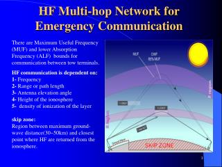
HF Inductors A NTENNA e.g. EPCOS Q-60 50 Ohm ± 10% Q = 10~30 F = 13.56 ± 200 kHz L3 res L2 L1 VSWR = 1 ~1.2 COAX HF Inductor C1 C2 C3 e.g. EPCOS Q-60 C4 VCC Component Value R1 1 20 RX_IN VDD_TX L4 2 19 C1 47pF C5 C6 VSS_RX TX_OUT R2 C2 10pF 3 18 R_MOD C3 10nF C8 4 17 C7 VDD_RX VSS_TX C4 47pF 5 16 C5 10µF Tantalum XTAL1 VCC XTAL 6 15 C6 100nF 13.56 MHz SCLOCK XTAL2 C7 22pF C9 7 14 M_ERR VSS_DIG C8 100nF 8 13 DIN XTAL_CLK C9 22pF µC 9 12 C10 100nF VCC VDD_DIG 10 11 L1 2.7µH DOUT L2 2.7µH C10 L3 5.6µH L4 3.3µH R1 2.2K Ohm R2 18 Ohm * * 18 Ohm = 20% Modulation (Recommended) 12 Ohm = 10% Modulation HF Multi-Protocol Transceiver IC Improved Matching Circuit
Xs1 Xs2 5 Ohm 50 Ohm RF Xp1 Xp2 • Matching circuit calculation: • Schematic of a double L matching circuit = T matching network
= = = W = W Q 40 f 13 , 56 Mhz Rs 5 Rl 50 ( ) = × + 2 R Rs Q 1 = × Xs 1 Q Rs Xs 1 = = m L 1 L 1 2 , 3 H × p × 2 f = × Xs 2 Q 2 Rl Xs 2 = = m L 2 L 2 7 , 4 H × p × 2 f × R R R Xp 2 Xp 1 = = - = = Xp 1 Q 2 1 Xp 2 Xp + Q Rl Q 2 Xp 2 Xp 1 = C 77 pF Calculation: R = Virtual resistance (instead of Xp1//Xp2) 1 = C × p × ƒ ×Xp 2
Caution: • Check the resonant frequency of the inductor! • Use only low tolerance components for the matching network to achieve optimum SWR! For Example: L1 and L2: +/-10% tolerance C2: +/-2% tolerance, temp. coefficient +-30ppm COG (Murata), Bad choice: Z5U material +22/-85% tolerance!!!
L3 L2 L1 COAX 1 to 10 Ohms C1 C2 C3 C4 VCC R1 1 20 RX_IN VDD_TX L4 Rd 2 19 C5 C6 VSS_RX TX_OUT R2 3 18 R_MOD C8 4 17 VDD_RX C7 VSS_TX 5 16 XTAL1 VCC XTAL 6 15 13.56 MHz SCLOCK XTAL2 C9 7 14 M_ERR VSS_DIG 8 13 DIN XTAL_CLK µC 9 12 VCC VDD_DIG 10 11 DOUT C10 • Suggested improvements to the application circuit: • Add a resistor between L4/C4 and TX_OUT/C3 • This action improves the EMC due to the decrease of the slew rate of the output MOS-FET.
Connect • Further decoupling of VCC and Interface lines with series resistance • Very cheap improvement regarding noise behavior • Split the receive and transmit ground-planes • Better de-coupling of receiver • Avoid using RS232 drivers that use switching frequencies in the range of 424 to 484 kHz or their harmonics (e.g. 141 kHz x 3 = 424 kHz)
15 SCLOCK 14 M_ERR 13 DIN µC 12 VCC VDD_DIG 11 DOUT 100nF 1nF Example (C10) • Add 1 nF ceramic capacitors in parallel to the C6, C8 and C10, 100 nF blocking capacitors at the IC VDD pins • These capacitors should be placed closest to the supply pins! • Ceramic capacitors have a much better HF noise filtering behavior due to their low inductance.
Tran1 switches the direction of SCLK Basic Request / Response ES1 = Reader EOF S1 and TAG commands generate a Reader SOF S2 indicates a TAG SOF ES2 indicates a TAG EOF data= to be sent to TAG Symbolic S1 cmd ES1 TRAN1 S2 TAG data ES2 TRAN2 Sclock Din Dout a b c d e f SCLK Host controller driven SCLK TAG driven • Basic communication structure:
First steps after assembly of a prototype board: 1. Check soldering and schematic 2. Switch on power supply and check supply voltages 3. Check timing! Minimum timings T1: 300ns T4: 600ns T2: 300ns T5: 300ns T3: 66ns T6: 300ns
SCLK DIN DOUT MERR 4. Read configuration register 0x71hex (MSB first) Result = 0x22(MSB first)
5.Write to configuration register 0x7Dhex(MSB first) SCLK DIN DOUT MERR Content = 0x27(MSB first) ISO 15693 / down link 1 out of 4, 100% modulation, one subcarrier (ASK) high data- rate (~26 kb), Manchester decoder disabled
6. Read configuration register 0x71hex(MSB first) SCLK DIN DOUT MERR Result = 0x27 (MSB first)
HF-ON Symbolic S1= Start ES1 = Stop Bit = 1 Sclock Din 7. Switch on HF: This operation must be performed first, otherwise SOF of the reader is not modulated properly.
8. Send a read TAG command (e.g. get Inventory) ISO Command Set:
0x2B (Command, Transceiver) ISO 15693, 1 out of 4, 100% modulation, FM, high data-rate 0x27, (Request flags): FM, high data-rate, use table 5 of ISO-spec, no protocol format extension, AFI not present, 1 slot, Option flag = 0, RFU = 0 (see ISO 15693-3 for details) 0x01, (Command, Tag): Inventory Command 0x00, Mask length: 0 0x2A, 0x50 : CCITT-CRC (Reverse, Start value 0xFFFF, 1’s compliment) Calculate CRC on these bytes Command string : 00101011 00100111 00000001 00000000 00101010 01010000 = 0x2B 0x27 0x01 0x00 0x2A 0x50 CRC 15693 Protocol Command LSB First MSB First 00101011 11100100 10000000 00000000 01010100 00001010 = 0x2B 0xE4 0x80 0x00 0x54 0x0A • Inventory Command Sequence:
CRC calculation: For the ISO 15693 tag protocols use: • CCITT-CRC, Byte entry, Reverse direction, Start value 0xFFFF, 1’s Complement For the Tag-it™ HF tag protocol use: • CCITT-CRC, Bit entry, Forward direction, Start value 0xFFFF, 1’s Compliment
TAG answer Inventory command DOUT HF SCLK MERR MERR pulse indicates that modulation on HF is finished Two zeroes are added to the TAG answer in front of EOF!
Register mode: Once the transceiver is initialized by the command byte in front of the data to be sent to the TAG, or by initializing the configuration register, the command byte does not need to be sent again, until the configuration needs changing again.
Set timing initialization: SCLK MERR DOUT HF 318,64 – 323,34 µs after the rising edge of EOF of the reader, theTAG should send its answer (ISO 15693-3).
The first scan pulse has to be in front of the first modulation pulse of the TAG! • Checking the Delay • Due to differences in the circuitry, it is possible, that there might be an additional delay in the answer. • If this occurs, the Manchester decoder of the Transceiver IC will not work properly anymore. • You can visualize the scan pulses of the Manchester decoder with following command sequence: 0x7B Data: 1100 0101 0110 0 (Boundary scan ON, Tdelay = 319 µs)
Timing offset [7 bits] Tdelay [µs] Minimum Value 306 µs 0000000 Typical 319 µs 0101100 Maximum Value 343 µs 1111111 Tdelay M_ERR • Solution - Change the Delay Example: 7 bits = 0101100 = 2C hex = 44dec 1 Bit equals 295 ns 44 x 295 = 12980nS = 13 µs Tdelay = 306 + 13 = 319 µs
Output power measurement: 22.8dBm = ~200mW
Transponder modulation measurement: Oscilloscope single turn aircoil TAG MODULATION DOUT SCLK
Antenna design: 1. Define and create Antenna Loop PCB or wire woundEquivalent circuit 2. Measure the inductance of the Loop
3. Calculate the components intermediate inductor, for calculation only! intermediate inductor, for calculation only!
4. Add variable (fixed) capacitors for fine tuning: • low tolerance components should be used – COG or NPO type capacitors • when optimum capacitor values have been found, the variable capacitors can be removed, • plan the space for 2 fixed, fine tuning capacitors at Cres and Cmatch
Resources Reference Guide (11-07-21-001) http://www.ti.com/tiris ISO/IEC 15693 Part 2/3 http://www.iso.ch ISO/IEC 14443 Part 2/3/4 http://www.iso.ch Antenna design notes http://www.ti.com/tiris/docs/manuals/appNotes/HFAntennaDesignNotes.pdf