Download
1 / 23
230 likes | 234 Views
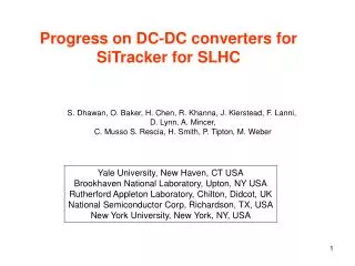
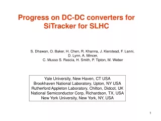
Yale University, New Haven, CT USA Brookhaven National Laboratory, Upton, NY USA Rutherford Appleton Laboratory, Chilton, Didcot, UK National Semiconductor Corp, Richardson, TX, USA New York University, New York, NY, USA. IEEE Nuclear Science Symposium, Orlando, FL USA 25-31 October, 2009.

E N D
Yale University, New Haven, CT USA Brookhaven National Laboratory, Upton, NY USA Rutherford Appleton Laboratory, Chilton, Didcot, UK National Semiconductor Corp, Richardson, TX, USA New York University, New York, NY, USA IEEE Nuclear Science Symposium, Orlando, FL USA 25-31 October, 2009
Length of Power Cables = 140 Meters 4088 Cables 3.5 V Cable Resistance = 4.5 Ohms 10 Chip Hybrid – SCT Module for LHC 10.25 V 1.5 amps Voltage Drop = 6.75 V Counting House 1.3 V 20 Chip Hybrid – Si Tr Module for Hi Luminosity 12.1V Voltage Drop = 10.8V 2.4 amps X 10 DC-DC Power Converter 1.3 V 13 V 20 Chip Hybrid – Si Tr Module for Hi Luminosity 14.08 V Voltage Drop = 1.08 V 2.4 amps 0.24 amps
Agenda • Learning from Commercial Devices • Buck > Voltage, EMI • Plug In Cards for ABCN2.5 Hybrids - Noise Tests @Liverpool • Require Radiation resistance & High Voltage operation • Thin Oxide • High Voltage with Thin Oxide ? • DMOS, Drain Extension 12V @ 5 nm , 20V @ 7 nm • HEMT has no Oxide – Higher Voltage ? 200 Mrads 20V
Synchronous Buck Converter 100 nsec 900 nsec 10 V 1 V
Enpirion EN5360 • Found out at Power Technology conference 0.25 µm Lithography • Irradiated Stopped on St. Valentines Day 2007 • No effects after 100 Mrads • Noise tests at Yale, RAL & BNL. • 20 µm Al is good shield for Air Coils • All other devices failed, even other part numbers from Enpirion • We reported @ TWEPP 2008 - IHP was foundry for EN5360 • What makes Radiation Hardness ? • Chinese Company Devices
What Makes it Rad Resistant ? Empirical Evidence: Deep submicron But what why?
What Makes it Rad Resistant ? We say thin Gate Oxide is a necessary Condition
Tunneling Region Thickness ~ 5 nm Oxide Trap Region + + + Fixed Charge States Switching Charge States V GND + + + + + Gate Oxide Si Book ‘Ionizing Radiation Effects in MOS Oxides’ Author Timothy R. Oldham
Can We Have High Radiation Tolerance & Higher Voltage Together ??? Controller : Low Voltage High Voltage: Switches – LDMOS, Drain Extension, Deep Diffusion etc >> 20 Volts HEMT GaN on Silicon, Silicon Carbide, Sapphire
LDMOS Structure Laterally Diffused Drain Extension High Voltage / high Frequency Main market. Cellular base stations High performance RF LDMOS transistors with 5 nm gate oxide in a 0.25 μm SiGe:C BiCMOS technology: IHP Microelectronics Electron Devices Meeting, 2001. IEDM Technical Digest. International2-5 Dec. 2001 Page(s):40.4.1 - 40.4.4
R. Sorge et al , IHP Proceedings of SIRF 2008 Conference High Voltage Complementary Epi Free LDMOS Module with 70 V PLDMOS for a 0.25 μm SiGe:C BiCMOS Platform
Enhancement Mode Normally OFF Depletion Mode Normally ON
Gallium Nitride Devices under Tests • RF GaN 20 Volts & 0.1 amp • 8 pieces: Nitronex NPT 25015: GaN on Silicon • Done Gamma, Proton & Neutrons • 65 volts Oct 2009 • 2 pieces: CREE CGH40010F: GaN on siC • 6 pieces: Eudyna EGNB010MK: GaN on siC • Done Neutrons Switch GaN • International Rectifier GaN on Silicon Under NDA Gamma: @ BNL Protons: @ Lansce Neutrons: @ U of Mass Lowell Plan to Expose same device to Gamma, Protons & Neutrons
200 Mrads of Protons had no effect – switching 20 V 0.1 Amp Parts still activated
Plug In Card with Shielded Buck Inductor Coupled Air Core Inductor Connected in Series 0.35 mm 1.5 mm Inductance ~ 0.6 µH 2.5 V @ 6 amps 12 V Spiral Coils Resistance in mΩ Replace pcb coil with copper foil
Hybrid in Thermal Shield Noise Same with Linear or DC - DC Shield 20 µm Al Foil Noise NO change with Plug in card on top Sensor 1 cm from Coil
IR’s basic current GaN-on-Si based device structure is a high electron mobility transistor (HEMT), based on the presence of a two dimensional electron gas (2DEG) spontaneously formed by the intimacy of a thin layer of AlGaN on a high quality GaN surface as shown in Figure 1. It is obvious that the native nature of this device structure is a HFET with a high electron mobility channel and conducts in the absence of applied voltage (normally on). Several techniques have been developed to provide a built-in modification of the 2DEG under the gated region that permits normally off behavior. Aside from providing high quality, reliable and a low-cost CMOS compatible device manufacturing process, the GaNpowIR technology platform also delivers dramatic improvements in three basic figures of merit (FOMs), namely specific on-resistance RDS(on), RDS(on)*Qg and efficiency*density/cost.
Conclusions • Learned from commercial Devices, Companies & Power conferences • Can get high Radiation Tolerance & Higher Voltage • High Frequency > Smaller Air coil > Less Material • Goal: ~20 MHz Buck, MEM on Chip size 9 mm x 9mm • Power SOC: MEMs Air Core Inductor on Chip • Study Feasibility 48 / 300V Converters • Irradiation: Run @ Max operating V & I. • Limit Power Dissipation by Switching duty cycle • Online Monitoring during irradiation for faster results • Yale Plug Cards can be loaned for Evaluation • Collaborators are Welcome
Working on Power Supply Is not Glamorous Neither it on Top of the World for ? More Details:www.Yale.edu/FASTCAMAC click on DC-DC