Download
1 / 1
10 likes | 139 Views
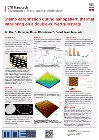
Stamp deformation during nanopattern thermal imprinting on a double-curved substrate. Jiri Cech a , Alexander Bruun Christiansen a , Rafael Josef Taboryski a. Results Submicron p atterns were transfered onto PMMA using PDMS stamp and onto PS using Zeonor foils. Conclusion

E N D
Stamp deformation during nanopattern thermal imprinting on a double-curved substrate Jiri Cecha, Alexander Bruun Christiansena, Rafael Josef Taboryskia Results Submicron patterns were transfered onto PMMA using PDMS stamp and onto PS using Zeonor foils. Conclusion Unit cell size have been characterized on stamp and on collected AFM data at deformation analysis points on polymer replica for 2 extreme cases, very thick and very thin PDMS soft stamp. • Motivation • Nanopatterning of double-curved surfaces remains to be great microfabrication challenge, but successful testing and control of such methods would allow various applications such as nanopatterning of injection mold cavities for low cost antireflective treatment of portable electronics optics. • Another application is surface wetting control on affordable medical devices. This would require good understanding of stamp deformation, including deformation on high curvature (low radius) surfaces. Cheng[1] created 600 nm pattern on curved surface with 57 mm radius, while an proximately 800 nm patterns was created by capillary force lithography on spherical substrate with 49 mm radius by Zhang[2] and Choi[3] used soft stamp to imprint 350 nm pattern on substrate with radius as little as 10 mm. There are two distinctly different stretching regimes, one for thick stamp and another for thickness comparable with height of curved substrate protrusion. However, results for combination of PS and Zeonor foils are more complex and not yet fully understood, primarily due to deformation of macrostructures and magnitude of XY anisotropy observed by AFM as shown. Confocal microscopy reconstructed surface image of spherical PS substrate surface after thermal imprinting with Zeonor COP foil. Pattern is optical grating. Method We used much higher curvatures (radius of 1.0 and 0.5 mm) to facilitate observation of bending and stretching of the employed soft stamps. We tested and compared 2 stamp materials, Silgard PDMS in two thicknesses and Zeonor COP foils 50, 100 and 188 um thick and 2 different polymer substrates, spun coated 350k PMMA and injection molded PS. Imprinted substrates have been characterized using laser scanning confocal microscopy, tapping mode AFM and SEM and pattern period was evaluated in different zones/regions of sample, using special software. Acknowledgment Project is funded by DTU Nanotech, the Danish National Advanced Technology Foundation (HTF), the Copenhagen Graduate School for Nanoscience and Nanotechnology (C:O:N:T). Surface tools have been manufactured by the Kaleido Technology ApS, polystyrene injection molding was done at InMoldBioSystems. AFM of nanopattern imprinted on spherical polymer substrate surface, average height of structures is 64 nm. Pattern is hexagonal array of pillars References [1] F. S. Cheng, S. Y. Yang, S. C. Nian, and L. A. Wang. Soft mold and gasbag pressure mechanism for patterning submicron patterns onto a large concave substrate. Journal of Vacuum Science & Technology B, 24(4):1724–1727, July-August 2006. [2] D. Zhang, W. Yu, T. Wang, Z. Lu, and Q. Sun. Fabrication of diffractive optical elements on 3-D curved surfaces by capillary force lithography. Optics Express, 18(14):15009–15016, July 2010. [3] W. M. Choi and O. O. Park. The fabrication of submicron patterns on curved substrates using a polydimethylsiloxane film mould. Nanotechnology, 15(12):1767–1770, December 2004. Positions of deformation analysis points and deformation of unsupported PS macrostructure. Jiri.Cech@nanotech.dtu.dk +45 61 79 29 00 345 Ørsteds Plads, 2800 Kgs. Lyngby Denmark