Download
1 / 17
180 likes | 337 Views
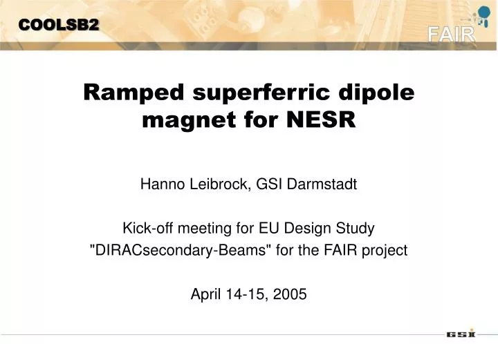
COOLSB2. Ramped superferric dipole magnet for NESR. Hanno Leibrock, GSI Darmstadt Kick-off meeting for EU Design Study "DIRACsecondary-Beams" for the FAIR project April 14-15, 2005. NESR in FAIR. FAIR Stage 1. versatile storage ring NESR. decelarated beams => ramped dipoles. Tasks.

E N D
COOLSB2 Ramped superferric dipole magnet for NESR Hanno Leibrock, GSI Darmstadt Kick-off meeting for EU Design Study "DIRACsecondary-Beams" for the FAIR project April 14-15, 2005
NESR in FAIR FAIR Stage 1 versatile storage ring NESR decelarated beams => ramped dipoles
Tasks EU FP6 task COOLSB2: superferric NESR-dipole for 1 T/s ramp rate Subtasks: • Magnet layout, yoke design • Superconducting coil design • Cryostat design => functioning prototype magnet
Dipole Parameters NESR Dipoles moderate field (<1.6 T), large aperture → superferric design Because • allows large apertures since the flux is guided by the iron and the field quality is defined by the pole shape, • field enhancement by the iron, • low operation costs challenges in red !
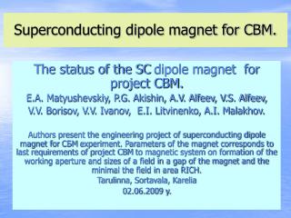
Preliminary 2D - design (by C. Muehle) Nuclotron cable 6000 A, 10 turns, 150 A/ mm2 (coil) curved (sagitta 69 mm)
SC coil design: choice of the conductor • ramp rate 1 T/s → low inductance needed → cable Rutherford cable CICC Nuclotron cable • eddy currents in helium containment (bobbin) and cryostat • → 'tube' forced-flow-cooling • → 'non'-conducting cryostat
Gantt diagram for R&D with milestones Milestones: Feasibility studies: December 31, 2005 Model cryostat delivered: June 30, 2006 Prototype dipole delivered: December 20, 2007
Conclusions • moderate field (<1.6 T), large aperture → superferric design (low operation costs) • ramp rate 1 T/s → low inductance needed → cable • a preliminary magnet design exists • the design of the cryostat has to make sure that eddy current effects are negligible • planned prototype dipole delivery: december 2007
Normal conducting CR-dipoles • Use of the same yoke for the normal conducting solution • => Problems: • Purcel filter -> loss of ampere turns • High flux density in yoke -> loss of ampere turns • Small coil window -> high current density • => 465kW power loss per magnet • Use of an appropriate (enlarged) yoke for the normal conducting solution • No purcel filter, but enlarged pole • Enlarged yoke for lower flux density • Enlarged coil window • => approx. 200kW power loss per magnet