Download
1 / 10
100 likes | 203 Views
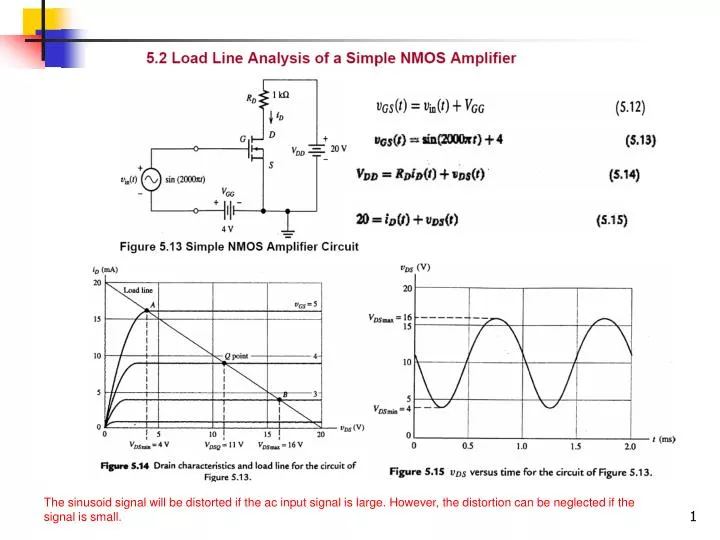
The sinusoid signal will be distorted if the ac input signal is large. However, the distortion can be neglected if the signal is small. Graphical solutions. Fig. 5.18. Small signal equivalent circuits. Assuming operation in the saturation region.

E N D
The sinusoid signal will be distorted if the ac input signal is large. However, the distortion can be neglected if the signal is small.
Small signal equivalent circuits Assuming operation in the saturation region For small signal case is negligible Where The gate current for FET is negligible gm = transconductance Small signal equivalent circuit Where,
Dependence of gm on Q-point and device parameters We know that and But from (5.3) Therefore μn- surface mobility of electron Cox- capacitance of gate per unit area
At higher frequencies small capacitance have to be added between device terminals • Also in the saturation region iD versus VDS is considered to be constant. This is not actually the case. The drain current, iD increases slightly as VDS increases. In order to take care of that we must add a drain resistance rd in the small signal model. More complex equivalent circuits
Determine the values of gm and rd the MOSFET characteristics shown below. From equation 5.34, we have, obtain iD = 6.7 mA at VDS = 4 V and iD = 8 mA at VDS = 14 V. Thus, the reciprocal of rd is calculated as: Example Thus, rd = 7.7 KΩ
C1, C2 – Coupling capacitors short circuit for AC signals and open circuit for DC bias calculation CS – bypass capacitor small impedance for AC Common source amplifier Voltage Gain (5.38) (5.39) (5.40) (5.41)