Download
1 / 1
10 likes | 126 Views
This work presents Deep N-well CMOS Monolithic Active Pixel Sensors as an innovative approach for signal processing in pixellated detectors in high-energy physics experiments. Various prototype MAPS with different resolutions have been developed in 130 nm triple well CMOS technologies. Experimental results, TCAD and Monte Carlo simulations have been used to study charge diffusion and sharing among pixels. The impact of front-end electronics on pixel fill-factor is explored, along with laser source tests and characterization of prototype chips. Simulation results and comparisons with experimental data are presented, showing promising outcomes for future MAPS development.

E N D
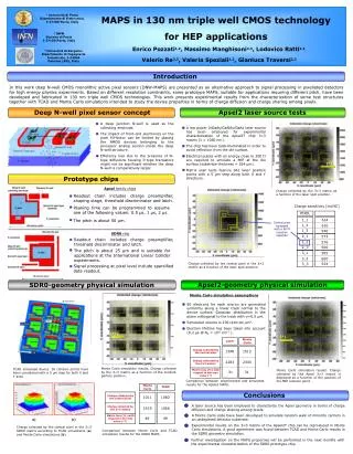
Introduction Charge sensitivity [mV/fC] PIXEL 614 1_1 1_2 610 1_3 540 2_1 573 2_2 576 2_3 500 3_1 565 3_2 600 3_3 534 1 Università di Pavia Dipartimento di Elettronica, I-27100 Pavia, Italy MAPS in 130 nm triple well CMOS technology for HEP applications 2 INFN Sezione di Pavia I-27100 Pavia, Italy Enrico Pozzati1,2,Massimo Manghisoni2,3, Lodovico Ratti1,2, Valerio Re2,3, Valeria Speziali1,2, Gianluca Traversi2,3 3 Università di Bergamo Dipartimento di Ingegneria Industriale, I-24044 Dalmine (BG), Italy In this work deep N-well CMOS monolithic active pixel sensors (DNW-MAPS) are presented as an alternative approach to signal processing in pixellated detectors for high energy physics experiments. Based on different resolution constraints, some prototype MAPS, suitable for applications requiring different pitch, have been developed and fabricated in 130 nm triple well CMOS technologies. This work presents experimental results from the characterization of some test structures together with TCAD and Monte Carlo simulations intended to study the device properties in terms of charge diffusion and charge sharing among pixels. Deep N-well pixel sensor concept Apsel2 laser source tests A deep junction N-well is used as the collecting electrode. The impact of front-end electronics on the pixel fill-factor can be limited by placing the NMOS devices belonging to the processor analog section inside the deep N-well structure. Efficiency loss due to the presence of N-type diffusions housing P-type transistors might not be significant whether the deep N-well is comparatively larger. A low power InGaAs/GaAlAs/GaAs laser source has been employed for experimental characterization of the Apsel2T chip 3×3 matrix (λ = 1060 nm). The chip has been back-illuminated in order to avoid reflection from the die surface. Electrical pulses with an energy close to 200 fJ are required to emulate a MIP at the die surface (substrate thickness = 254 µm). Matrix scan tests fearure 961 laser position points with a 5 µm step along both X and Y directions. (*) Prototype chips Apsel family chips Charge collected by the 3×3 matrix as a function of the laser spot position. Readout chain includes charge preamplifier, shaping stage, threshold discriminator and latch. Peaking time can be programmed to assume one of the following values: 0.5 µs, 1 µs, 2 µs. The pitch is about 50 µm. Central pixel equipped with a 60 fF injection capacitor SDR0 chip Readout chain includes charge preamplifier, threshold discriminator and latch. The pitch is about 25 µm and is suitable for applications at the International Linear Collider experiments. Charge collected by the central pixel in the 3×3 matrix as a function of the laser spot position. Signal processing at pixel level include sparsified data readout. Apsel2-geometry physical simulation SDR0-geometry physical simulation Monte Carlo simulation assumptions 80 electrons for each micron are generated uniformly along a linear track normal to the device surface. Gaussian distribution in the plane orthogonal to the track with σ=0.5 µm. Simulated volume is 230×230×80 µm3. Electron lifetime has been taken into account (9.2 µs @ NA = 1015 cm-3 ). (**) (*) Monte Carlo Laser Charge collected by the central pixel 1398 1512 Charge collected by the 3×3 matrix 2283 2343 Monte Carlo simulation results. Charge collected by the 3×3 matrix as a function of the incident particle position. TCAD simulated device. 36 collision points have been considered with a 5 µm step for both X and Y axes. Monte Carlo simulation results. Charge collected by the Apsel 3×3 matrix is displayed as a function of the position of the MIP collision point. Matrix loss (%) with respect to the max value (*) 31 31 Comparison between experimental and simulated results for the Apsel2 MAPS. Monte Carlo TCAD Conclusions Charge collected by the central pixel 1011 1060 A laser source has been employed to characterize the Apsel geometry in terms of charge diffusion and charge sharing among pixels. Charge collected by the 3×3 matrix 1619 1566 A Monte Carlo code have been developed to simulate random walk of minority carriers in an undepleted detector substrate. Matrix loss (%) with respect to the max value (**) 48 49 a) b) Experimental results on the 3×3 matrix of the Apsel2T chip can be reproduced in Monte Carlo simulations. A good agreement was found between TCAD and Monte Carlo results in the SDR0 geometry simulation. Charge collected by the central pixel in the 3×3 SDR0 matrix according to TCAD simulations (a) and Monte Carlo simulations (b). Comparison between Monte Carlo and TCAD simulation results for the SDR0 MAPS. Further investigation on the MAPS properties will be performed in the next months with the experimental characterization of the SDR0 prototype chip.