Download
1 / 9
90 likes | 118 Views
Learn about the impact of lattice defects on the energy levels of electrons in semiconductors, including non-stoichiometric compositions, substitutional defects, vacancies, and more. Explore doped semiconductors, charge carrier concentrations, and the Hall effect.

E N D
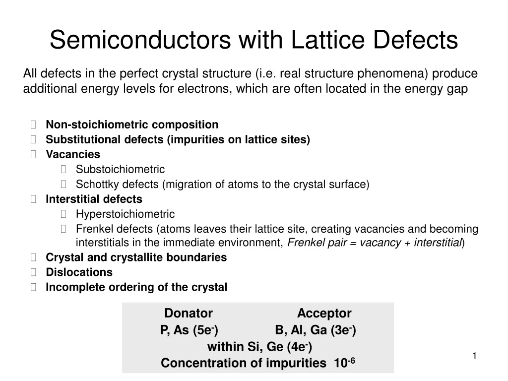
Semiconductors with Lattice Defects All defects in the perfect crystal structure (i.e. real structure phenomena) produce additional energy levels for electrons, which are often located in the energy gap • Non-stoichiometric composition • Substitutional defects (impurities on lattice sites) • Vacancies • Substoichiometric • Schottky defects (migration of atoms to the crystal surface) • Interstitial defects • Hyperstoichiometric • Frenkel defects (atoms leaves their lattice site, creating vacancies and becoming interstitials in the immediate environment, Frenkel pair = vacancy + interstitial) • Crystal and crystallite boundaries • Dislocations • Incomplete ordering of the crystal Donator Acceptor P, As (5e-) B, Al, Ga (3e-) within Si, Ge (4e-) Concentration of impurities 10-6
Doped (extrinsic) Semiconductors Additional „conduction electrons“ (with P, As) Additional holes (with Ba, Al, Ga) p-type semiconductors with electron acceptors (B, Al, Ga) n-type semiconductor with electron donors (P, As)
Fermi Energy in Doped Semiconductors n-type semiconductor At 0K the Fermi energy is located between the new energy band and E0. At high temperatures, the Fermi energy approaches the value , as in intrinsic semiconductors. Largest differences in electrical properties are expected at low temperatures (< 400K). In p-type semiconductors, the temperature dependency is reversed
Number of Charge Carriers (per units of volume) and Electrical Conductivity Small concentration of impurities • Large concentration of impurities • (b) Small concentration of impurities
The Hall Effect Semiconductor (or metal) within an external magnetic field Without magnetic field: The concentration of electrons along the y-direction is homogeneous Within a magnetic field: The movement of electrons is affected by the Lorentz force, causing a non homogeneous distribution of electrons along the y-direction and the formation of an electric field Lorentz force: Hall force: Equilibrium: Hall constant: The sign of Hall constant is different for n and p.
The IV, III-V and II-VI Semiconductors IV Si: Fd3m, a = 5,430 Å Ge: Fd3m, a = 5,657 Å III-V GaAs: F-43m, a = 5,653 Å GaAs: P63mc, a = 3,912 Å, c = 6,441 Å InAs: F-43m, a = 6,056 Å GaSb: F-43m, a = 6,095 Å InSb: F-43m, a = 6,487 Å GaN: P63mc, a = 3.189 Å, c = 5.185 Å II-VI CdTe: F-43m, a = 6,481 Å
The IV, III-V and II-VI Semiconductors C: Fd3m, a = 3.567 ÅGe: Fd3m, a = 5.657 Å Si: Fd3m, a = 5.430 Å-Sn: Fd3m, a = 6.489 Å GaAs: F-43m, a = 5.653 Å InAs: F-43m, a = 6.056 Å InSb: F-43m, a = 6.487 ÅGaP: F-43m, a = 5.450 Å SiC: F-43m, a = 4.358 Å ZnO: P63mc, a = 3.254 Å, c = 5.210 ÅCdSe: P63mc, a = 4.297 Å, c = 7.007 Å