DSP Board
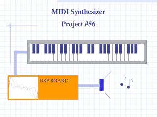
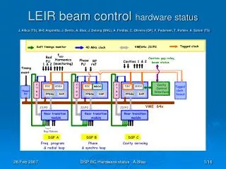
LEIR beam control hardware status J. Allica (TS), M-E Angoletta, J. Bento, A. Blas, J. Delong (BNL), A. Findlay, C. Oliveira (OP), F. Pedersen, T. Rohlev, A. Salom (TS). DSP Board. 6 unit VME board with:

DSP Board
E N D
Presentation Transcript
LEIR beam control hardware statusJ. Allica (TS),M-E Angoletta, J. Bento, A. Blas, J. Delong (BNL), A. Findlay, C. Oliveira (OP), F. Pedersen, T. Rohlev, A. Salom (TS) DSP BC Hardware status A.Blas
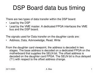
DSP Board 6 unit VME board with: 1 DSP - ADSP-21160M from Analog Devices – 32 bit floating point – Super Harvard Architecture (SHARC), Clocked at 80 MHz (40 MHz external), 600 MFLOPS - with separate data and instruction busses, dedicated I/O processor with separate bus - 64 bit external data bus clocked at 40 MHz (320 MB/s), 6 byte link Ports at 80 MHz (80 MB/s), 2 serial ports at 40 Mbits/s. 1 MB Flash memory, to restore the DSP software. 4 MB DSP RAM, to store external or calculated functions (like voltage and rf program, steering …) 4 daughter board sites, with two 69 pin connectors for each site 1 Timing interface, based on an AlteraTM FPGA 1 VME interface, based on an AlteraTM FPGA 1 Data interface, based on an AlteraTM FPGA that controls the data flux on Board. 4 MB RAM, for acquisition of internal signals (diagnostics) 16 Trigger inputs (via the RTM) 1 Event link, basically a serial link connected to the rear transition module that allows taking into account 256 events with a hundred ns resolution (not used at CERN). 6 link ports, each portallows up to 8 bit data transfer per DSP internal clock cycle (80 MHz) DSP BC Hardware status A.Blas
MDDS Master DDSdaughter card Designed in November 2004 AD9858 1GHz clock DDS ADF4106 PLL + CLV1000A VCO (10MHz => 1 GHz) No SRAM Altera Stratix EP1S10F484C5 2 Tagged clock outputs with IEEE1394 mechanical standard Tagging inside the FPGA with external ELMEC 1.2ns delay (needs control of logical cells placement) DSP BC Hardware status A.Blas
IEEE 1394b clock distribution 1.5 ns tag 333 Ms/s equivalent throughput Standard used up to 3.2 Gb/s over 5m cables 9 pin connector LVDS electrical standard 1394b bilingual connector 8 x 5 mm DSP BC Hardware status A.Blas
Clock Fan-out VME card Designed in June 2005 1 input with IEEE1394 mechanical standard 1 Optical input / 1 optical output 9 outputs IEEE1394 Delay error between channels below 390 ps DSP BC Hardware status A.Blas
DDC Digital Down Converterdaughter card 4 channel 14 bit ADC AD 9245BCP-80 (80 MHz max) NEW (since July 2005): 2 MB/10 ns (instead of 500k/12ns) SRAM (1 M x 16 bits) Altera Stratix EP1S20F484C5 (instead of EP1S10) 1 Tagged clock input with IEEE1394 mechanical standard and de-tagging and divide-by-2 circuit (50% duty cycle and minimum pulse width required by the ADC). DSP BC Hardware status A.Blas
DDC Digital Down Converterdaughter card – FPGA interconnections DSP BC Hardware status A.Blas
DDC Digital Down Converterdaughter card – FPGA content 1 channel / 4 • 4 down mixers with 4 different LO frequencies • Programmable CIC, 0 -> 3 stages, 1 ->15 decimation, 1 -> 255 comb delay, normalization gain • CIC, FIR and LO parameters loaded synchronously with a specific double-tag. Allows on-flight MDDS harmonic change • I/Q frequency discriminator • LO frequency measurement (counter) • 4 different acquisition lines memorizing 4 of 28 different inner signals. Sampling at a chosen sub-harmonic of the main clock. Up to 1 M points per signal at a maximum sampling of 80 MHz. • Channel, CIC, FIR ON/OFF • Reset phase accumulator at each tag DSP BC Hardware status A.Blas
DDCQuartus Compilation With only 2/4 LO’s and 2nd order FIR !
SDDS Slave DDSdaughter card 4 channel 14 bit DAC AD 9754BCP-80 (125 MHz max) NEW (since July 2005): 2 MB/10 ns (instead of 500k/12ns) SRAM (1 M x 16 bits) Altera Stratix EP1S20F484C5 (instead of EP1S10) 1 Tagged clock input with IEEE1394 mechanical standard and de-tagging and divide-by-2 circuit (50% duty cycle and minimum pulse width required by the ADC). High/Low DAC gain (0 – 18 dB) 17 bit DAC for lowest amplitude signals DSP BC Hardware status A.Blas
SDDS Slave DDSdaughter card • 4 up-converters with 4 different LO frequencies • LO parameters loaded synchronously with a specific double-tag. Allows on-flight MDDS harmonic change • LO frequency measurement (counter) • 4 different acquisition lines memorizing 4 of 28 different inner signals. Sampling at a chosen sub-harmonic of the main clock. Up to 1 M points per signal at a maximum sampling of 80 MHz. • Channel ON/OFF • Reset phase accumulator at each tag • Automatic DAC gain setting with respect to required output amplitude • Phase modulation from SRAM DSP BC Hardware status A.Blas
RTM Rear Transition ModuleVME card Designed in June 2005 16 trigger lemo inputs - to VME P2 connector - or outputs - from P2 connector of CTRV board via two 16-wire flat cables and special board (top right of this page) - direction selected by bridge for each pair) of DSP board or 8 link port connectors VME P2 connector DSP BC Hardware status A.Blas
CCI Cavity Control InterfaceNIM card Interfaces the SDDS and the 2 LEIR cavities (14-pin flat cable to the SDDS) Makes the sum of 2 harmonics for each cavity Disable the rf out when the cavity is not ready DSP BC Hardware status A.Blas
Possible Upgrades • DSP Board: light upgrade. Study achieved by Tony (bug fixes + VME-DSP bus decoupling). The cards need to be produced and tested + FPGAs programmed => 5 man-weeks + 3 kCHF • version 2: requirements being written by ME Angoletta. VME bus isolation + JTAG remote programming + more FPGA and DSP power. 12 man-weeks + 12kCHF • DDC: FPGA upgrade to have 4 LO’s instead of 2 and FIR filter. 6 man-weeks + 8 kCHF DSP BC Hardware status A.Blas
Stock DSP BC Hardware status A.Blas
PS test BC implementation DSP BC Hardware status A.Blas