Download
1 / 34
340 likes | 457 Views
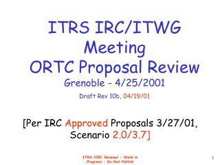
[Per IRC Approved Proposals 3/27/01, Scenario 2.0/3.7]. ITRS IRC/ITWG Meeting ORTC Proposal Review Grenoble - 4/25/2001 Draft Rev 10b, 04/19/01. S=0.7 [0.5x per 2 nodes]. Pitch. Gate. MOS Transistor Scaling (1974 to present). 0.7x. 0.7x.

E N D
[Per IRC Approved Proposals 3/27/01, Scenario 2.0/3.7] ITRS IRC/ITWG Meeting ORTC Proposal Review Grenoble - 4/25/2001 Draft Rev 10b, 04/19/01 ITRS 2001 Renewal - Work in Progress - Do Not Publish
S=0.7 [0.5x per 2 nodes] Pitch Gate MOS Transistor Scaling(1974 to present) ITRS 2001 Renewal - Work in Progress - Do Not Publish
0.7x 0.7x 250 -> 180 -> 130 -> 90 -> 65 -> 45 -> 32 -> 22 -> 16 0.5x N N+1 N+2 Scaling Calculator ITRS 2001 Renewal - Work in Progress - Do Not Publish
ITRS Approved Scenario Proposal (3/27/00 Telecon) Scenarios 2.0(DRAM), 3.7(MPU), 3.x (ASIC/Low Power*) the DRAM Half-pitch (HP) should remain on a 3-year-cycle trend after 130nm/2001 (Sc 2.0). • the MPU HP may be on a 2-year-cycle trend until 90nm/2004, and then remain equal to DRAM HP Sc 2.0 on a 3-year cycle (Sc 3.7). • the MPU (HP) Printed (PrGL) and Physical (PhGL) Gate Length will be on 2-year-cycle trends until 45nm and 32nm, respectively, at year 2005, and then parallel to the DRAM/MPU HP trends on a 3-year cycle (Sc 3.7). • the ASIC/Low Power* HP/GL to be negotiated and added by Taiwan/Europe/Japan IRC/TWGs at Grenoble 4/26,27 ITRS meetings. [*Note: ASIC/Low Power Half-pitch and Gate Lengths may lag “most aggressive” MPU High-Performance HPs/GLs by 1-2 years] ITRS 2001 Renewal - Work in Progress - Do Not Publish
Scenario 2.0/DRAM 3.7/MPU (2-yr cycle M/A HP & G.L. <2005; 3yr >2005) ITRS Roadmap Acceleration Continues... 95 97 99 01 04 07 10 13 16 500 500 2-Year Node Cycle 1995-2001 Sc 3.7 MPU Half-Pitch (1-year Lag Thru 2002, then equal to DRAM after 2004) 350 350 250 250 (DRAM Half Pitch) Technology Node 180 180 1998/1999 DRAM Half-Pitch MPU/ASIC 130 130 Feature Size (nm) 2000 Update, Sc 2.0 Gate Length 100 100 XX Technology Node - DRAM Half-Pitch (nm) Minimum 90 DRAM Sc 2.0 = 3-yr cycle after 2001 70 XX 70 Feature Size 65 50 XX 50 45 35 MPU/ASIC Gate XX In Resist “ ” 1999 ITRS 35 32 25 XX 25 22 16 95 97 99 01 04 07 10 13 16 ~.7x per 11 Year of Production technology 2001 Renewal Period “Most Aggressive” Sc 3.7 = 2-yr<’05; 3-yr >’05 MPU Printed (PrGL) & Physical (PhGL) Gate Length cycle node (.5x 8.0 per 2 nodes) ITRS 2001 Renewal - Work in Progress - Do Not Publish
2001 Renewal ORTC DRAM and MPU Technology Node Tables 1a,b [ITRS Typical Table Header Format ] ITRS 2001 Renewal - Work in Progress - Do Not Publish
2001 Renewal ORTC ASIC Technology Node Tables 1aa,ba [ITRS ASIC/Low Power Chapter Table Header Format ] ITRS 2001 Renewal - Work in Progress - Do Not Publish
Samsung @ ISSCC/Feb2001: 4Gb DRAM, 645mm2, [0.15u2 ave cell area] (ITRS: 0.13u2/2001) 2000 Update [Sc. 2.0/3.7] [Approved for use in 2001 Renewal w/MPU Sc. 3.7] DRAM Chip size - 2000 ITRS ORTC Update Proposal [Sc. 2.0] ITRS 2001 Renewal - Work in Progress - Do Not Publish
800mm2 Litho Field Size 572mm2 Litho Field Size 286mm2 2 per Field Size 310mm2 340mm2 170mm2 Sc 3.7: Flat Thru 2004 85mm2 42mm2 MPU Chip size - 2000 ITRS ORTC Update Proposal [ Sc. 2.0 vs 3.7 ] ITRS 2001 Renewal - Work in Progress - Do Not Publish
SRAM A-Factors for Simple 6T SRAM Cell using Microprocessor Logic CMOS Process Technology ‘94-’00 Historical A-factor Reduction Rate Ave = 0.967x = -3.3% CAGR [1999 ITRS Target: -7% CAGR**] Average A-Factor = 161.67 ‘98-’00 Historical A-factor Reduction Rate Ave = 0.913x = -8.7% CAGR Cell Size (u2) 2.43 u2 2.48 u2 5.59 u2 10.3 u2 20.5 u2 15.8 u2 ** 1.2x/4yrs “affordable” MPU chip size growth; @ 2x/2yrs Transistors/chip Function Growth; @ 0.5x/3yrs Technology Node (f) Reduction ITRS 2001 Renewal - Work in Progress - Do Not Publish
ITRS Chip Size Model Proposal: Sc 2.0/DRAM [no change]; Sc 3.7/MPU Proposal: Li = MPU 4t Gate; Ai = ASIC 4t Gate; Si = 6t SRAM cell; St = SRAM transistor L S L Li L Li Li L S Li Ai Ai Si Li Si St Ai S St Li St Si Ai S St Si Li Ai St Si Ai Li Si St Ai Li Si St Ai Si St Ai St Si = ASIC Gate (4t) , eSRAM (6t) (Design TWG) Chip Function Density Trend Chart - ITRS Proposal 3.7 ITRS 2001 Renewal - Work in Progress - Do Not Publish
Sc 3.7 - w/Innovation* : 2x/2yrs Non-Gate-Length Performance Innovation* 1999 ITRS 9.6Ghz/11nm 25Ghz/4.2nm 4.8Ghz/22nm 2.4Ghz/45nm 1.2Ghz/90nm 3.4Ghz/32nm .6 Ghz/180nm 1.7Ghz/65nm 2023 2011 .3 Ghz/350nm 2001 2005 Sc 3.7 w/o Innov.*:1999- 2005 Freq = 2x/4yrs ; GL = .71x/2yr 2005- 2016 Freq = 2x/6yrs ; GL = .71x/3yr Historical: Freq = 2x/2yrs ; GL = .71x/yr 1995 1999 1997 2003 2008 2014 Log Frequency MPU Max Chip Frequency - ITRS GL Proposal Sc 3.7 ITRS 2001 Renewal - Work in Progress - Do Not Publish
ITRS Table Definitions/Guidelines - 2001Proposal Rev0, 10/02/00 [As Presented in IRC/Taiwan 12/06/01] • Technology Requirements Perspective - Near-Term Years : First Yr. Ref.+ 6 yrs F’cast (ex. 2001 through 2007), annually - Long-Term Years : Following 9 years (ex.: 2010, 2013, and 2016), every 3 years • Technology Node : - General indices of technology development. - Approximately 70% of the preceding node, 50% of 2 preceding nodes. - Each step represents the creation of significant technology progress - Example: DRAM half pitches: 130, 90, 65, 45, 32, 22, 16 nm -Smallest 1/2 pitch among DRAM, ASIC, MPU, etc • Year of Production: - The volume = 10K units (devices)/month. ASICs manufactured by same process technology are granted as same devices - Beginning of manufacturing by a company and another company starts production within 3 months • Technology Requirements Color: - : Manufacturable Solutions are NOT known - : Manufacturable Solutions are known - : Manufacturable Solutions exist, and they are being optimized - Red cannot exist in the next three years (2002, 2003, 2004) ** - Yellow cannot exist the next year (2002) ** White Red Yellow ** Exception [By Review/Approval of IRC]: Solution NOT known, but does not prevent Production manufacturing ITRS 2001 Renewal - Work in Progress - Do Not Publish
Backup: • DRAM Chip Size Model (Sc. 2.0) • MPU Chip Size Model (Sc. 3.7) • Scenario GraphsHistory; Sc 2.0; Sc 2.0’; Sc 3.0; Sc 4.0; Sc 3.5 • Fabless Semi Assoc. (FSA) Node Roadmap • Backup Articles • UMC 130nm/70nm ; • IEDM; • EUV Consortium; • Samsung 90nm Litho; • Samsung 4Gb ISSCC • Roadmap Definitions/Guidelines ITRS 2001 Renewal - Work in Progress - Do Not Publish
History, incl. 2000 Update Sc 2.0 and Node Corrections ITRS Roadmap Acceleration Continues... (Including MPU/ASIC “ Physical Gate Length) 95 97 99 01 04 07 10 13 16 500 500 1994 350 350 250 250 (DRAM Half Pitch) Technology Node 1997 180 180 1998/1999 MPU/ASIC 130 130 2000 Update, Sc 2.0 Feature Size (nm) Gate Length 100 100 XX Technology Node - DRAM Half-Pitch (nm) Minimum 90 70 XX 70 Feature Size 65 50 XX 50 45 35 MPU/ASIC Gate “In Resist” 1999 ITRS XX 35 32 33 MPU/ASIC Gate “Physical” 2000 Update 25 “ ” XX 25 22 23 16 95 97 99 01 04 07 10 13 16 ~.7x per Year of Production technology 2001 Renewal Period node (.5x per 2 nodes) ITRS 2001 Renewal - Work in Progress - Do Not Publish
Sc 2.0 (1-yr DRAM HP Node pull-in; .7x Node Trend correction; 1-yr PhG.L. Lead) ITRS Roadmap Acceleration Continues... (Including MPU/ASIC “ Physical Gate Length”) 95 97 99 01 04 07 10 13 16 500 500 Samsung 01/30/01 Press Release: 90nm H.P./1G DRAM - 2002 ‘04 2-Year Node Cycle 1995-2001 350 350 250 250 (DRAM Half Pitch) Technology Node 180 180 1998/1999 MPU/ASIC 130 130 2000 Update, Sc 2.0 Feature Size (nm) Gate Length 100 100 XX Technology Node - DRAM Half-Pitch (nm) Minimum 90 70 XX 70 Feature Size 65 50 XX 50 45 35 XX MPU/ASIC Gate “In Resist” 1999 ITRS 35 32 33 MPU/ASIC Gate “Physical” 2000 Update 25 XX 25 22 23 16 95 97 99 01 04 07 10 13 16 ~.7x per Year of Production technology 2001 Renewal Period node (.5x per 2 nodes) ITRS 2001 Renewal - Work in Progress - Do Not Publish
Sc 2.0’ (PrG.L = .7 x DRAM HP; 1-yr PhG.L. lead) ITRS Roadmap Acceleration Continues... 95 97 99 01 04 07 10 13 16 500 500 2-Year Node Cycle 1995-2001 350 350 250 250 (DRAM Half Pitch) Technology Node 180 180 1998/1999 MPU/ASIC 130 130 2000 Update, Sc 2.0 Feature Size (nm) Gate Length 100 100 XX Technology Node - DRAM Half-Pitch (nm) Minimum 90 70 XX 70 Feature Size 65 50 XX 50 45 35 MPU/ASIC Gate XX In Resist “ ” 1999 ITRS 35 32 MPU/ASIC Gate “Physical” 2000 Update;“In Resist” Sc 2.0’ 25 “ ” XX 25 22 23 MPU/ASIC Gate “Physical” Sc 2.0’ 16 95 97 99 01 04 07 10 13 16 ~.7x per Year of Production technology 2001 Renewal Period node (.5x per 2 nodes) ITRS 2001 Renewal - Work in Progress - Do Not Publish
ITRS Roadmap Acceleration Continues... 95 97 99 01 04 07 10 13 16 500 500 350 350 250 250 (DRAM Half Pitch) Technology Node 180 180 1998/1999 MPU/ASIC 130 130 2000 Update, Sc 2.0 Feature Size (nm) Gate Length 100 100 XX Technology Node - DRAM Half-Pitch (nm) Minimum 90 3-Year Node Cycle DRAM, M/A HP > 2001 70 XX 70 Feature Size 65 50 XX 50 2-yr G.L. pull-in Scenario 3.0 45 35 MPU/ASIC Gate XX In Resist “ ” 1999 ITRS 35 32 25 XX 25 22 12/00 Press Releases: 130nm H.P./70nm G.L. - 2001 16 95 97 99 01 04 07 10 13 16 ~.7x per 11 Year of Production technology 2001 Renewal Period node (.5x Sc 3.0 per 2 nodes) Scenario 3.0 (2-yr G.L. Pull-in); 3-yr Node/G.L. cycle 2-Year Node Cycle 1995-2001 ITRS 2001 Renewal - Work in Progress - Do Not Publish
Scenario 4.0 (2-yr FSA* Node Goals), Sc 3.5 (1-yr lag M/A HP, G.L.) FSA* Node Goals MPU/ASIC Half-Pitch (1-year Lag) ITRS Roadmap Acceleration Continues... FSA* Feb ‘01 Presentation: “Fabless” Semiconductor / Foundry Goals for Logic H.P: 180nm/2000; 130nm/2002 90nm/2004; 65nm/2006 95 97 99 01 04 07 10 13 16 500 500 2-Year Node Cycle 1995-2001 350 350 250 250 (DRAM Half Pitch) Technology Node FSA* Feb ‘01 Presentation: “Fabless” Semiconductor / Foundry Goals for Nodes: 180nm/1999; 130nm/2001 90nm/2003; 65nm/2005 180 180 1998/1999 MPU/ASIC 130 130 2000 Update, Sc 2.0 Feature Size (nm) Gate Length 100 100 XX *FSA = “Fabless” Semiconductor Association Technology Node - DRAM Half-Pitch (nm) Minimum 90 70 XX 70 Feature Size 65 50 XX 50 45 35 MPU/ASIC Gate XX In Resist “ ” 1999 ITRS 35 32 25 XX 25 22 12/00 Press Releases: 130nm H.P./70nm G.L. - 2001 16 95 97 99 01 04 07 10 13 16 ~.7x per 11 Year of Production technology 2001 Renewal Period node (.5x 12/00 IEDM demo: 65nm H.P./32nm PrG.L. “2005 into mfg” per 2 nodes) ITRS 2001 Renewal - Work in Progress - Do Not Publish
MPU/ASIC Half-Pitch (1-year Lag) ITRS Roadmap Acceleration Continues... FSA* Feb ‘01 Presentation: “Fabless” Semiconductor / Foundry Goals for Logic H.P: 180nm/2000; 130nm/2002 90nm/2004; 65nm/2006 95 97 99 01 04 07 10 13 16 500 500 2-Year Node Cycle 1995-2001 350 350 250 250 (DRAM Half Pitch) Technology Node Samsung 01/30/01 Press Release: 90nm H.P./1G DRAM - 2002 ‘04 180 180 1998/1999 DRAM Half-Pitch MPU/ASIC 130 130 2000 Update, Sc 2.0 Feature Size (nm) Gate Length 100 100 XX Technology Node - DRAM Half-Pitch (nm) Minimum 90 70 XX 70 Feature Size 65 50 XX 50 45 35 MPU/ASIC Gate XX In Resist “ ” 1999 ITRS 35 32 25 XX 25 22 12/00 Press Releases: 130nm H.P./70nm G.L. - 2001 16 95 97 99 01 04 07 10 13 16 ~.7x per 11 Year of Production technology 2001 Renewal Period DRAM Sc 2.0/3.5 = 3-yr node (.5x 12/00 IEDM demo: 65nm H.P./32nm PrG.L. “2005 into mfg” 8.0 per 2 nodes) “Most Aggressive” Sc 3.5 = 2-yr; M/A H.P.;MPU Pr&Ph G.L. cycle 5.5 Scenario 3.5 (1-yr Lag, 2-yr cycle M/A HP, G.L.) ITRS 2001 Renewal - Work in Progress - Do Not Publish
Scenario 2.0/DRAM 3.7/MPU (2-yr cycle M/A HP & G.L. <2005; 3yr >2005) MPU Half-Pitch (1-year Lag Through 2002, then equal to DRAM) ITRS Roadmap Acceleration Continues... FSA* Feb ‘01 Presentation: “Fabless” Semiconductor / Foundry Goals for Logic H.P: 180nm/2000; 130nm/2002 90nm/2004; then 3-yr cycle 95 97 99 01 04 07 10 13 16 500 500 2-Year Node Cycle 1995-2001 350 350 250 250 (DRAM Half Pitch) Technology Node Samsung 01/30/01 Press Release: 90nm H.P./1G DRAM - 2002 ‘04 180 180 1998/1999 DRAM Half-Pitch MPU/ASIC 130 130 2000 Update, Sc 2.0 Feature Size (nm) Gate Length 100 100 XX Technology Node - DRAM Half-Pitch (nm) Minimum 90 3-Year Node Cycle Sc 3.7 MPU HP > 2004 70 XX 70 Feature Size 65 50 XX 50 45 35 MPU/ASIC Gate XX In Resist “ ” 1999 ITRS 35 32 25 XX 25 22 12/00 Press Releases: 130nm H.P./70nm G.L. - 2001 16 95 97 99 01 04 07 10 13 16 ~.7x per 11 Year of Production technology 2001 Renewal Period DRAM Sc 2.0/3.7 = 3-yr node (.5x 12/00 IEDM demo: 65nm H.P./32nm PrG.L. “2005 into mfg” 8.0 per 2 nodes) “Most Aggressive” Sc 3.7 = 2-yr<’05; 3-yr >’05 MPU H.P.; MPU PrG.L. & PhG.L. cycle ITRS 2001 Renewal - Work in Progress - Do Not Publish
Moving from 8 inch to 12 inch wafers gives you 125 percent more chips. Source: “From Criticized to Respected to Preferred” Presentation, , 2/06/01 - Fabless Semiconductor Association (FSA) Website, Author: Jodi Shelton, FSA Executive Director <<http://www.fsa.org/resources/history2.ppt>> Technology Acceleration:Foundry Lead ITRS 2001 Renewal - Work in Progress - Do Not Publish
Note: 2005 65nm Half Pitch Isol. Line = 35nm PrGL; 32nm PhGL “Fabless” Foundries: 1-yr cycle FSA “Node Goals” - Sc 4.0: 2-yr cycle continues 2-yr cycle 2.0-yr cycle continue? ‘07/65nm ITRS Sc. 2.0: 1-yr cycle 2-yr cycle 3-yr cycle Moving from 8 inch to 12 inch wafers gives you 125 percent more chips. Source: “From Criticized to Respected to Preferred” Presentation, , 2/06/01 - Fabless Semiconductor Association (FSA) Website, Author: Jodi Shelton, FSA Executive Director <<http://www.fsa.org/resources/history2.ppt>> Technology Acceleration:Foundry Lead ITRS 2001 Renewal - Work in Progress - Do Not Publish
“Logic HP LEAD” FSA Node Goals - Sc 4.0 “Actual” Logic Half-Pitch (1-Year Lag) - Sc 3.5 “Actual” Logic Half-Pitch Forecast: 2002/130nm; 2006/65nm (2-yr cycle) Moving from 8 inch to 12 inch wafers gives you 125 percent more chips. Source: “From Criticized to Respected to Preferred” Presentation, , 2/06/01 - Fabless Semiconductor Association (FSA) Website, Author: Jodi Shelton, FSA Executive Director <<http://www.fsa.org/resources/history2.ppt>> Technology Acceleration:Foundry Lead ITRS 2001 Renewal - Work in Progress - Do Not Publish
“... UMC plans 70nm gates using phase-shifting and 248nm lithography Semiconductor Business News (01/18/01 15:09 p.m. PST) “...Plans to ramp production of 0.07µm (70-nanometer) physical gate-length transistors for processor-class products, using phase-shifting mask (PSM) technology from Numerical Technologies with its 0.13µm logic process with existing 248nm deep UV lithography tools, starting later this year in 200mm fabs. Will use for processors with transistor switching speeds <9 picoseconds. Chose PSM route because 193nm litho tools would not be production ready for MPU-class gate lengths under 100 nm. UMC WorldLogic 0.13µm process technologies Gate-length Application 0.12µm 120nm very low leakage devices 0.10µm 100nm low leakage devices 0.09µm 90nm standard speed devices 0.07µm 70nm microprocessors (MPUs) ...” “UMC plans 70nm gates using phase-shifting and 248nm lithography”Semiconductor Business News (01/18/01 15:09 p.m. PST) ITRS 2001 Renewal - Work in Progress - Do Not Publish
<http://www.siliconstrategies.com/semibiznews/ OEG20001215S0001> “...Semiconductor manufacturers may be years away from their coveted goal of developing a high-k gate dielectric that will replace silicon dioxide and meet future performance and power-consumption targets, even as SiO2 is reaching its limits, according to researchers at IEDM. Intel set the tone for the gate-oxide scaling debate - researcher Robert Chao said transistors with 30-nm[32] LG, and a gate oxide of just 8Å (0.8-nm), conceivably could be made in 2005, when the 70-nm[65] technology node moves into manufacturing….” “Chip makers under pressure to develop high-k dielectric”- EE Times Article 12/15/00 ITRS 2001 Renewal - Work in Progress - Do Not Publish
“..Ultimately (in the 2005 time frame) we will manufacture microprocessors based on 30-nanometer [32] transistors, and EUV lithography will be a critical component of that manufacturing process. The processors that result from this will operate at around10GHz…EUV lithography is scheduled to support IC manufacturing at the 70-nanometer [65]technology node. This requires preproduction tools for process development in late 2003 or early 2004 and production tools in 2005…” (Cnet interview with Charles Gwyn, general manager and program director of the Extreme Ultraviolet LLC consortium) *For more... http://news.cnet.com/news/0-1014-201-4822673-0.html “10 gigahertz or bust”(Cnet- Feb 15, 2001) ITRS 2001 Renewal - Work in Progress - Do Not Publish
< http://www.siliconstrategies.com/story/OEG20010130S0011 > “...Samsung said the photoresist enables mass production of 1-Gbit memories with 0.09-micron [02?]and below design rules [‘04 per IRC, 2/26/01 telecon] [Sc. 2.0 1G: ISSCC/Intro(180nm, 400mm2)/1999; Production(100nm, 157mm2)/2003] ....The 193-nm resist is expected to enable device shrinks down to the 0.07-micron level, according to Samsung…. [Sc. 2.0: 130nm/01, 115nm/02; 100nm/03, 90nm/04;70nm/06, 65nm/07; 50nm/09, 45nm/10; 35nm/12, 32nm/013; 25nm/15, 22nm/016] … The company said it eventually plans to use the new compound and193-nm scanners to produce 64-Gbit DRAMs with ArF lithography…” [Sc. 2.0 64G:ISSCC(57nm-45nm, 1200-800mm2)/2008-10; Intro(35-32nm, 450-400mm2)/2012-13; Production(25-22nm, 300-250mm2)/2015-16] “Samsung targets 1-Gb DRAM production in '02 using new 193-nm resist”(Semiconductor Business News -01/30/01) ITRS 2001 Renewal - Work in Progress - Do Not Publish
“ISSCC: Samsung Reveals 4Gbit DDR SDRAM Prototype”(Electronic News - Feb, 2001) Samsung Electronics Co. Ltd. has busted the DRAM density barrier with a prototype DDR SDRAM chip that has four times as many transistors as anything ever made before, according to the Korea-based company. Samsung engineers have managed to squeeze more than 4 billion transistors onto a single chip, said Hongil Yoon, a senior Samsung engineer, today at the ISSCC in San Francisco. The chip uses a twisted open bitline architecture, and measures a whopping 645 square millimeters, or 1 square inch [25.4mm square, 0.150u2 ave cell area x .90 (est. cell area efficiency) = 0.135 cell area; using “0.10u design rule”* => a=15; versus ITRS 2000 Update: a=8, f=0.13u, af^2 = 0.135 in 2001]. *For more... http://www.electronicnews.com/enews/news/6222-38NewsDetail.asp ITRS 2001 Renewal - Work in Progress - Do Not Publish
Rev 6 ITRS Scenario Proposal -Scenario 3.5 MPU/ASIC Half-pitch Correction • Additional careful evaluation of the Fabless Semiconductor Association (FSA) Sc 4.0 Node goals suggests that the actual MPU/ASIC (M/A) half-pitch should lag the FSA Node goals by 1 year. This is more consistent historically [2-year lag, accelerating to a 1-year lag, crossing over in future (2005) per conclusions at the Taiwan ITRS meeting]. • Therefore, please review an attached proposal M/A Sc 3.5 table line items for a more correct proposal for the M/A half-pitch and the associated M/A Sc 3.5 Printed (PrGL) and Physical (PrGL Gate Lengths. • For continuity, additional graphs are included to show the progression from Sc 2.0 -> Sc 2.0’ -> Sc 3.0 -> Sc 4.0(FSA Node Goals) -> M/A Sc 3.5 • Also included are the FSA Node Roadmap w/ Sc 3.5 M/A half-pitch analysis and the • other collateral backup articles reviewed at the 2/26 (Asia) and 2/28 (Eur) IRC Teleconferences. ITRS 2001 Renewal - Work in Progress - Do Not Publish
ITRS Table [2000 Update] Definitions/Guidelines, Proposal Rev1, 7/11/00 [As Presented in 2000 Update/Taiwan 12/06/01] • Technology Requirements Perspective - Near-Term Years : First Yr. Ref.+ 6 yrs F’cast (ex. 1999 through 2005), annually - Long-Term Years : Following 9 years (ex.: 2008, 2011, and 2014), every 3 years • Technology Node : - General indices of technology development. - Approximately 70% of the preceding node, 50% of 2 preceding nodes. - Each step represents the creation of significant technology progress - Example: DRAM half pitches (2000 ITRS) of 180, 130, 90, 65, 45 and 33 nm *Year 2000 : Smallest 1/2 pitch among DRAM, ASIC, MPU, etc • Year of Production: - The volume = *10K units (devices)/month. ASICs manufactured by same process technology are granted as same devices - Beginning of manufacturing by *a company and another company starts production within 3 months • Technology Requirements Color : - : Manufacturable Solutions are NOT known - : Manufacturable Solutions are known - : Manufacturable Solutions exist, and they are being optimized *Year 2000 : Red cannot exist in next 3 years (2000, 2001, 2002)** *Year 2000 : Yellow cannot exist in next 1 year (2000) White Red Yellow ** Exception: Solution NOT known, but does not prevent Production manufacturing ITRS 2001 Renewal - Work in Progress - Do Not Publish
[Sc. 2.0/3.7] Sc 2.0/3.7: DRAM Will Continue to Lead Half-Pitch Nodes[DRAM 3-yr HP after 2001, MPU HP 2-yr-cycle through 2004, then 3-yr-cycle; MPU GL 2-yr-cycle GL through 2005; ASIC/Lo-Power HP/GL Line Items to be developed and added at Grenoble 4/26,27/2001] Sc 2.0/DRAM, 3.0/MPU Approved @ 2/26 IRC Telecon; Sc 3.7 Approved by IRC Review 3/27/01 97 98 99 00 01 02 03 04 05 06 07 08 09 10 11 12 13 14 15 16 DR HP 1.5 250 180 130 100 90 70 65 50 45 35 32 25 DR HP 2.0 250 210180 150 130 115 100 90 80 70 65 60 50 45 40 35 32 30 25 22 FSA HP 4.0250 210180 150 130 105 90 75 65 M/A HP 1.5350 180 130 100 90 70 65 50 45 35 32 25 M/A HP 2.0350 230 160 130 100 90 70 65 50 45 35 32 M/A HP 3.0350 280220 180 150 130 115 100 90 80 70 65 60 50 45 40 35 32 30 25 MPU HP 3.7400 255 215 180 150 130 105 90 80 70 65 60 50 45 40 35 32 30 25 22 Sc 1.5 Pr 200 100 90 75 65 50 45 35 32 25 22 18 16 7/00 Ph 200 120 100 75 65 50 45 35 32 25 22 18 16 13 Sc 2.0 Pr 200 140 100 90 70 65 50 45 35 32 25 22 18 7/00 Ph 200 120 100 90 70 65 50 45 35 32 25 22 18 16 Sc 2.0’Pr 180 100 90 70 65 50 45 35 32 25 22 18 16 11/00 Ph 180 100 90 70 65 50 45 35 32 25 22 18 16 Sc 3.0 Pr 180 150120 100 90 75 65 60 50 45 40 35 32 30 25 22 20 18 16 15 12/00 Ph 180 135 100 90 75 65 60 50 45 40 35 32 30 25 22 20 18 16 15 13 Sc 3.7 Pr180 150 130 105 90 75 65 53 45 40 35 32 30 25 22 20 18 16 1513 MPU Ph 180 130 90 75 65 53 45 37 32 30 25 22 20 18 16 15 13 11 10 9.0 Sc 2.0/DRAM, 3.7/MPU Approved 3/27 Rev 8, 3/27/01 ITRS 2001 Renewal - Work in Progress - Do Not Publish


![[Per IRC Approved Proposals 3/27/01, Scenario 2.0/3.7; Plus DesTWG MPU Chip Model Proposal ]](https://cdn1.slideserve.com/2958869/per-irc-approved-proposals-3-27-01-scenario-2-0-3-7-plus-destwg-mpu-chip-model-proposal-dt.jpg)