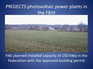
Download
1 / 28
280 likes | 298 Views
HelioVolt Corporation aims to develop and commercialize efficient, safe, reliable, and affordable thin-film photovoltaic solar power products that enable energy production at cost parity with conventional sources of electricity. Their mission includes achieving low cost, long durability, and high efficiency in their solar power products.

E N D
HelioVolt Corporation:The Future of Photovoltaic Power B.J. StanberyHelioVolt Corporation 8201 E. Riverside Dr., Suite 600Austin, TX 78744 Energy Technology & Policy B.J. Stanbery, HelioVolt Corporation
Cost Durability Efficiency HelioVolt Mission • To develop and commercialize a new generation of efficient, safe, reliable, and attractive thin-film photovoltaic solar power products that are the first to enable energy production at cost parity with conventional sources of electricity. • Lowest cost thin film circuits, less than one fourth that of silicon PV and one tenth that of current Building Integrated PV (“BIPV”) products • Warranted Lifetime of at least 20 years for first products • Comparable conversion efficiencies to multicrystalline silicon Energy Technology & Policy B.J. Stanbery, HelioVolt Corporation
Solar Power Learning Curve • Plateau in direct manufacturing costs • Data source Luuk Beurskens, ECN Policy Studies, PHOTEX’03 Energy Technology & Policy B.J. Stanbery, HelioVolt Corporation
Lifetime Required for 10¢/kW·h Energy at Various Module Costs Energy Technology & Policy B.J. Stanbery, HelioVolt Corporation
Solar Power Yesterday • Silicon Photovoltaic (PV) modules for retrofit • PV module sales $5.5B (2005) • PV market 30+% CAGR since ‘97, +40% 2005 • Sales <½% total annual global CapEx for electrical power generation • Current market limited by supply, even at price of • $4/Wp modules + $3 installation = $7/Wp Energy Technology & Policy B.J. Stanbery, HelioVolt Corporation
Over $1 in silicon materials cost dominates COGS Data source Prog.Photovolt.Res.Appl. 5, 309-315(1997) Silicon Module Limitations $1.78/Wp projected lowest costfor crystalline Si PV modules Energy Technology & Policy B.J. Stanbery, HelioVolt Corporation
Semiconductor Cost Reduction Energy Technology & Policy B.J. Stanbery, HelioVolt Corporation
Solar Power Tomorrow • Power Buildings will become multi-$T market • PV as an integrated electronic component • Efficient, durable thin-film solar cells incorporated into traditional building materials • Current products unsuitable for this market Energy Technology & Policy B.J. Stanbery, HelioVolt Corporation
Electrical Demand met by PV Power Buildings Market • Huge latent demand • USA potential:$150B/yr • 60% share • Multiple segments • Architectural glass • Windows & skylights • Roofing Energy Technology & Policy B.J. Stanbery, HelioVolt Corporation
Precursor 1 Reactive Transfer Printing Printing Plate Precursor 2 Stage 1: Precursors’ Deposition Substrate Printing Plate Mechanical (& Electrostatic) Pressure Heat Stage 2: Rapid Thermal Processing and Separation Product Layer Substrate Micro-Reactor Energy Technology & Policy B.J. Stanbery, HelioVolt Corporation
CIGS PV Device Semiconductor: Copper Indium Gallium Diselenide • Highest efficiency single-junction thin-film PV semiconductor material • 19.5% conversion efficiency (NREL) • Unique material properties derive from spontaneous nanostructuring • Inherently stable under normal operating conditions • Second generation photovoltaic semiconductor material Energy Technology & Policy B.J. Stanbery, HelioVolt Corporation
RTP Implementation: FASST ™ CIGS Semiconductor Synthesis • Field-Assisted Simultaneous Synthesis and Transfer • Second generation CIGS manufacturing technology • Advantages • Rapid processing • Vastly reduced thermal budget • Confinement of volatile selenium • Electrostatic field effects on ionic constituent transport during synthesis Energy Technology & Policy B.J. Stanbery, HelioVolt Corporation
Rapid Thermal Processor Electrostatic Chuck Printing Plate Printing Plate Release Layer Printing Plate Precursor 2 Release Layer Precursor 2 Release Layer Precursor 1 Metal Contact Layer Precursor 1 Substrate Metal Contact Layer Substrate emitter CIGS CIGS Metal Contact Layer Metal Contact Layer Substrate Substrate Completed Device FASST ™ Process Sequence Flash Heating Recoat Printing Plate Device Processing Energy Technology & Policy B.J. Stanbery, HelioVolt Corporation
First Factory Production Flow Metal Pattern (P1) Glass Clean 1. Front End Metal Deposition PrecursorDeposition 3. Buffer BufferDeposition FASST ™ Synthesis 2. CIGS Synthesis Absorber Pattern (P2) TCODeposition TCO Pattern (P3) 4. Device Processing Product Packaging Test & Ship 5. Back End Energy Technology & Policy B.J. Stanbery, HelioVolt Corporation
CIGS Thin-Film Products • CIGS is an alloy of Copper, Indium, Gallium and Selenium • Monolithic integration forms circuits without high wafer assembly costs • CIGS is one of three known intrinsically stable PV materials (with Silicon and Gallium Arsenide) • Instrinsic stability required for long lived robust products • More efficient absorber of light than any other known semiconductor • Requires 1/100th of the material compared to silicon for comparable light absorption Energy Technology & Policy B.J. Stanbery, HelioVolt Corporation
Product Value Proposition Revolutionary FASSTTM Manufacturing Process CIGS Thin-Film Technology HelioVolt Thin-Film PVICs • Highest performance; most versatile & durable • PVIC platform avoids costly inter-cell wiring & bypass components • Proven semiconductor CIGS (Copper Indium Gallium Selenide) • Lowest Cost Thin Film Devices • Less than 1/4th the cost of silicon PV module • Integrated systems for Power Buildings less than1/10th cost of current technologies • Lower cost electricity than effective current retail electricity prices in five years • Wide Range of Applications for both rigid and flexible PVIC platform products • Traditional PV modules • Building Integrated PV (BIPV) Systems Energy Technology & Policy B.J. Stanbery, HelioVolt Corporation
Reactive Transfer Printing (RTP) • Combines features of • Rapid Thermal Annealing, and (optionally) • Anodic Wafer Bonding • electrostatic fields effects • Advantages • Rapid processing • Eliminates pre-reaction • Independent pre-heating of precursors • Confinement of volatile species • Independent precursor deposition optimization Energy Technology & Policy B.J. Stanbery, HelioVolt Corporation
Rapid Thermal Annealing (RTA) • RTA is a non-equilibrium thermal processing method widely used in semiconductor device manufacturing • Often used to provide activation energy whilst minimizing concomitant diffusion • Employed for formation and annealing of gate dielectric layers in FET’s • Used for reactive formation of electrical contacts by thermal silicidation of silicon/metal interfaces Energy Technology & Policy B.J. Stanbery, HelioVolt Corporation
Metal Selenization Coevaporation HelioVoltFASST™ CIGS Film Process Time • Rapid processing delivers high capital efficiency Energy Technology & Policy B.J. Stanbery, HelioVolt Corporation
Thermal Budget Comparison • One to three orders of magnitude reduction in thermal budget Figure of Merit (FOM) • Highest average processing temperature Energy Technology & Policy B.J. Stanbery, HelioVolt Corporation
Anodic Wafer Bonding (AWB) • AWB is widely used for MEMS manufacture • Employs electrostatic fields to bond alkali glass to semiconductors or metals with lower temperature and pressure than fusion bonding • High voltage across the wafer/glass stack repels mobile ions in the glass, inducing a space-charge and creating strong electrostatic compression, pulling them into intimate contact on an atomic scale. Energy Technology & Policy B.J. Stanbery, HelioVolt Corporation
Electrostatic Compression • HelioVolt’s FASST™ CIGS process utilizes both mechanical and electrostatic compression • Length scale is much smaller than conventional AWB Energy Technology & Policy B.J. Stanbery, HelioVolt Corporation
CIGS Precursor Deposition Methods • Low-temperature vacuum deposition • Provides increased throughput compared to conventional high-temperature CIGS synthesis by co-deposition or selenization • Non-vacuum liquid precursor deposition • HelioVolt/NREL Cooperative Research & Development Agreement (CRADA) • Goal: development of non-vacuum nanomaterial-based precursor deposition processes • Synthesis of CIGS demonstrated using FASST™ processing • Details to be presented by Jennifer Nekuda at the Fall 2007 MRS meeting in Boston later this month Energy Technology & Policy B.J. Stanbery, HelioVolt Corporation
Recrystallization of Nanoscale Granular Precursor Films • FASST™ CIGS cross-section Precursor Film Energy Technology & Policy B.J. Stanbery, HelioVolt Corporation
Composition Fluctuations and Carrier Transport in CIGS PV Absorbers • Peculiar semiconductor behavior: Copper Indium Gallium Selenide (CIGS) PV devices insensitive to extended defects and ±5% atomic composition variations of its metallic constituents • Selenium deficiency results in poor devices • Observations • CIGS PV devices are always copper deficient compared to a-CuInSe2 • Compositions lie in the equilibrium a+b 2-phase domain Energy Technology & Policy B.J. Stanbery, HelioVolt Corporation
Composition Fluctuations and Carrier Transport in CIGS PV Absorbers • Experimental results* HAADF-TEM & nano-EDS • 5-10 nm characteristic domain size (2-D) • Pearson product-moment statistical correlation between the two variables Cu/(In+Ga) and Ga/(In+Ga) is 0.72 (null P=0.3% ) *Applied Physics Letters, 87, 2005, 121904 Energy Technology & Policy B.J. Stanbery, HelioVolt Corporation
Reactive Transfer Printing for Film Synthesis • RTP is an advanced printing method for making films and coatings. It offers • Low thermal budget • Confinement of volatile reaction components • Electrostatic modification of ionic transport • FASST™ implementation of RTP is a processing method with demonstrated capabilities to • Utilize nano-particle based precursors for high-quality CIGS synthesis • Modify nanodomain formation during CIGS synthesis Energy Technology & Policy B.J. Stanbery, HelioVolt Corporation
HelioVolt Corporation:The Future of Photovoltaic Power B.J. StanberyHelioVolt Corporation 8201 E. Riverside Dr., Suite 600Austin, TX 78744 Energy Technology & Policy B.J. Stanbery, HelioVolt Corporation