Download
1 / 25
250 likes | 394 Views
E. Atkin , E . Malankin , V. Shumikhin NRNU MEPhI , Moscow. Analog front-end chip for GEM detectors. GEM Chip structure Channels structure Test benches E xperimental data Summary. OUTLINE. GEM detectors. ~50 µm. C ross -section of a triple GEM detector.

E N D
E. Atkin, E.Malankin, V. Shumikhin NRNU MEPhI, Moscow Analogfront-endchipfor GEM detectors
GEM • Chipstructure • Channelsstructure • Testbenches • Experimentaldata • Summary OUTLINE
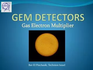
GEM detectors ~50 µm Cross-section of a triple GEM detector P. Abbon et al. / NIM (2007) 455–518
CBM Muon system of the internationalCBM experiment, being designed on the new accelerator facilities at FAIR GSI (Darmstadt, Germany), built on the base of the gaseous detector of high resolution. Muon System consists of about 1 million channels. For the Muon System signals read-out ASIC application is neccesary.
CBM Muon system of the internationalCBM experiment, being designed on the new accelerator facilities at FAIR GSI (Darmstadt, Germany), built on the base of the gaseous detector of high resolution. Muon System consists of about 1 million channels. For the Muon System signals read-out ASIC application is neccesary.
CBM ~1 millionchannels ↓ ~15 000 ASICsx 64 ch. Muon system of the internationalCBM experiment, being designed on the new accelerator facilities at FAIR GSI (Darmstadt, Germany), built on the base of the gaseous detector of high resolution. Muon System consists of about 1 million channels. For the Muon System signals read-out ASIC application is neccesary.
CBM ~1 millionchannels ↓ ~15 000 ASICsx 64 ch. Front-endfor MUCH Muon system of the internationalCBM experiment, being designed on the new accelerator facilities at FAIR GSI (Darmstadt, Germany), built on the base of the gaseous detector of high resolution. Muon System consists of about 1 million channels. For the Muon System signals read-out ASIC application is neccesary.
Input signal range of 1.5-100 fC • Chargepolarity – negative • ENC – less than 0.3 fC • Detectorcapacitance up to 100 pF • Maximum hit rate/channel – 2 MHz • Power consumption – 2 mW/ch SPEcifications
CHIP sTRUCTURE 5 CSA + standaloneShaperchannels (Preampver. 1) 5 CSA channelwithbuilt-inshaping (Preampver. 2) OpAmpblock Digitalteststructures
CSA COre • Inputtransistor – • nMOS (7mm*360 nm) • Common source stage • Folded boost current amplifier • Output source follower Feedback: gain setting cap + discharge transistor to set the maximumhit rate of channel not less than 2MHz
SHAPER Noninverting 2nd order Sallen-Key filter The shaper has two additional adjustments: - TAIL – tail cancellation - SH_BL – baselinetuning
Preampver.2 • Inputtransistor – • nMOS (4mm *360 nm) • Common source stage • Folded boost current amplifier • Output source follower Feedback: gain setting cap + discharge resistor to set the maximumhit rate of channel not less than 2MHz
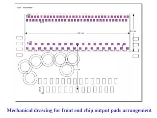
CHIP Layout • CLCC68 Package • Die–1525 x 1525 μm2 • UMC 180 nmCMOS MMRF process • 2012 run ofEuropractice
Testboard LDO regulator 1 pFcapacitance CLCC Socket Detectorcapacitanceemulation
Testboard Referencepotentiometers LDO regulator 1 pFcapacitance CLCC Socket Detectorcapacitanceemulation
OUTPUT RESPONSES (ver.1) Input charge swept from 25 to 70 fC Shaper CSA Voltagepulser CSA CSA & Shaper
TRANSFER FUNCTION (ver.1) Shaper Channelgain ~ 6 mV/fC • Dynamicrange – 1.5 – 100 fC • Integralnolinearity ~ 4% CSA CSA gain ~ 2.5 mV/fC
RMS NOISE MEASURMENTS (ver.1) Aim: Cin >> Cdet Estimation: CSA open-loop gain ≥ 1400
CSA OUTPUT RESPONSE & Transferfunctionver.2 CSA output transferfunction CSA gain ~ 5 mV/fC
NOISE ESTIMATION • PreAmp (ver. 1) • ENC – 875е Cdet = 1p • 2427e Cdet = 100p • PreAmp (ver. 2) • ENC – 1070е Cdet = 1p • 2500e Cdet = 100p
Testboardwith GEM* GEM Anode Padarea 5x5 mm2 Padcapacitance 12 pF SocketwithChip GaschamberwithAr/CO2 *TestboarddesignedbyPNPIteam
TESTS WITH 55Fe source* • 55Fe amplitudespectrum, obtainedbythepreamplifier & GEM. • Preamplifieroutput *testsprovidedbyPNPIteam
SUMMARY Designedandprototyped 2 versionsofread-outwithpreliminary CBMMUCH specifications: