Download
1 / 82
840 likes | 1.1k Views
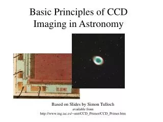
Basic Principles of CCD Imaging in Astronomy. Based on Slides by Simon Tulloch available from http://www.ing.iac.es/~smt/CCD_Primer/CCD_Primer.htm. What is a CCD?. “CCD” = “Charge-Coupled Device” Invented in 1970s, originally for: Memory Devices Arithmetic Processing of Data

E N D
Basic Principles of CCD Imaging in Astronomy Based on Slides by Simon Tulloch available from http://www.ing.iac.es/~smt/CCD_Primer/CCD_Primer.htm
What is a CCD? • “CCD” = “Charge-Coupled Device” • Invented in 1970s, originally for: • Memory Devices • Arithmetic Processing of Data • When Made of Silicon (Si), has same Light-Sensitive Properties as Light Meters • Use them to “Measure” Light • Applied to Imaging as Sensor
CCDs in Astronomy • Revolutionized Astronomical Imaging • More Sensitive than Photographic Emulsions • Factor of 100 Measure Light only 0.01 as Bright • Improved Light-Gathering Power of Telescopes by nearly 100 • Amateur w/ 15-cm (6") Telescope + CCD can get similar performance as 1960s Professional with 1-m (40") Telescope + Photography • Now Considered to be “Standard” Sensor in Astronomical Imaging • Special Arrangements with Observatory Now Necessary to use Photographic Plates or Film
What is a CCD? • Made from Crystalline Material • Typically Silicon (Si) • CCD Converts “Light” to “Electronic Charge” • Spatial Pattern of Light Produces a Spatial Pattern of Charge = “Image” • “Digitized” • Analog Measurements (“Voltages”) Converted to Integer Values at Discrete Locations • Stored as Computer File
Regular Pattern of Si atoms Fixed Separations Between Atoms Atomic Structure Pattern “Perturbs” Electron Orbitals Changes Layout of Available Electron States from Model of Bohr Atom Si Crystal Structure http://www.webelements.com/webelements/elements/text/Si/xtal.html
- - - - Electron States in Si Crystal • Available States in Crystal Arranged in Discrete “Bands” of Energies • Lower Band Valence Band • More electrons • Upper Band Conduction Band • Fewer electrons • No States Exist in “Gap” Between Bands Conduction Band of Electron States Increasing energy “Gap” = 1.12 electron-volts (eV) “Gap” Valence Band of Electron States
Comparison of State Structure in Crystal with Bohr Model Conduction Band Orbitals Valence Band “Gap” States “Blur” Together To Form “Bands” Discrete Transition Single Atom in Crystal Isolated Atom (as in Gas)
Action of Light on Electron States • Incoming Photon w/ Energy 1.12 eV Excites Electrons From “Valence Band” to “Conduction Band” • Electron in Conduction Band Moves in the Crystal “Lattice” • Excited Electron e-leaves “Hole” (Lack of Electron = h+) in Valence Band • Hole = “Carrier” of Positive Charge
Action of “Charge Carriers” • Carriers are “Free” to Move in the Band • Electron e- in Conduction Band • Hole h+ in Valence Band • Charge Carriers may be “Counted” • Measurement of Number of Absorbed Photons
Maximum to “Jump” Si Band Gap • 1 eV = 1.602 10-12 erg = 1.602 10-12 Joule To Energize Electron in Si Lattice Requires < 1.1 m
Energy and Wavelength • Incident Wavelength > 1.1 m Photon CANNOT be Absorbed! • Insufficient Energy to “Kick” Electron to Conduction Band Silicon is “Transparent” to long CCDs constructed from Silicon are Not Sensitive to Long Wavelengths
After Electron is Excited into Conduction Band…. • Electron and Hole Usually “Recombine” Quickly • Charge Carriers are “Lost” • Apply External Electric Field to “Separate” Electrons from Holes • “Sweeps” Electrons Away from Holes • Maintains Population of “Free” Electrons • Allows Electrons to be “Counted”
Hole Electron Generation of CCD Carriers photon photon Conduction Band Valence Band
Spontaneous Recombination photon photon Conduction Band Valence Band
+ + + + Prevent Spontaneous Recombination by Applying Voltage to “Sweep” Electrons + Ammeter
Prevent Spontaneous Recombination by Applying Voltage to “Sweep” Electrons + + + + + Ammeter
Thermal “Noise” • Big BUT: Other Kinds of Energy Have Identical Effect • Thermally Generated Electrons are Indistinguishable from Photon-Generated Electrons • Heat Energy can “Kick” e- into Conduction Band • Thermal Electrons appear as “Noise” in Images • “Dark Current” • Keep CCDs COLD to Reduce Number of Thermally Generated Carriers (Dark Current)
How Do We “Count” Charge Carriers (“Photoelectrons”)? • Must “Move” Charges to an “Amplifier” • Astronomical CCDs: Amplifier Located at “Edge” of Light-Sensitive Region of CCD • Charge Transfer is “Slow” • Most of CCD Area “Sensitive” to Light • Video and Amateur Camera CCDs: Must Transfer Charge QUICKLY • Less Area Available to Collect Light
“Bucket Brigade” CCD Analogy • Electron Charge Generated by Photons is “Transferred” from Pixel to “Edge” of Array • Transferred Charges are “Counted” to Measure Number of Photons
Rain of Photons VERTICAL COLUMNS of PIXELS BUCKETS (PIXELS) MEASURING CYLINDER (OUTPUT AMPLIFIER) CONVEYOR BELT (SERIAL REGISTER)
Rain of Photons Shutter
Empty First Buckets in Column Into Buckets in Conveyor Belt MEASURING CYLINDER (OUTPUT AMPLIFIER) CONVEYOR BELT (SERIAL REGISTER)
MEASURING CYLINDER (OUTPUT AMPLIFIER) CONVEYOR BELT (SERIAL REGISTER)
Empty Second Buckets in Column Into First Buckets
Empty Third Buckets in Column Into Second Buckets
After each bucket has been measured, the measuring cylinder is emptied, ready for the next bucket load. Measure & Drain
Measure & Drain
Empty First Buckets in Column Into Buckets in Conveyor Belt Now Empty
Empty Second Buckets in Column Into First Buckets
Measure & Drain
Measure & Drain
Measure & Drain
Empty First Buckets in Column Into Buckets in Conveyor Belt