Download
1 / 21
210 likes | 304 Views
Learn about the layout of large transistors, output drivers, buffering, and ESD protection in CMOS circuits. Discover principles behind tri-state drivers, latch-up triggers, and avalanche punch-through protection.

E N D
Buffering S = scaling or tapering factor CL = SN+1 Cg ……………… All inverters have identical delay of to = delay of the first stage (load =Cd+Cg)
5 S 4 3 0 1 2 3 Cd/Cg Buffering If the diffusion capacitance Cd is neglected, S = e = 2.7
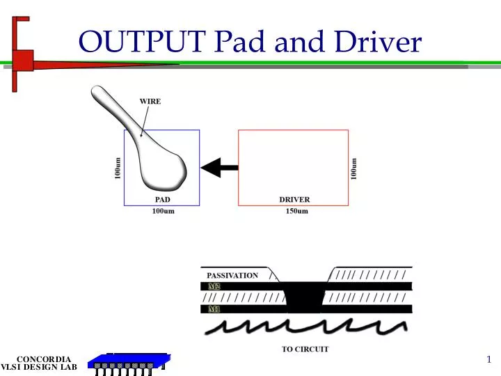
Output Drivers Standard CMOS Driver Open Drain/Source Driver: Single Transistors Tri-state Driver Bi-directional Circuit
Tri-state Driver V DD En Out In En • Tri-state or High impedance • Used to drive internal or external busses • Two inputs: • Data In and Enable • Various signal assertions • Two types: • C2MOS • CMOS with Control Logic C2MOS
Tri-state Driver V Control logic could be modified to obtain Inversion/non-inversion Active low/high Enable For large load, pre-drivers are required DD En PAD Out En In
Latch-up: Trigger • Factors which trigger latch-up • transmission line reflections or ringing • voltage drop on the VDD bus • “hot plug in” of unpowered circuit board • electrostatic discharge • sudden transient on power and ground busses • leakage current across the junction • radiation: x-ray, cosmic
Protection Circuitry Principles Avalanche Punch Through
Input protection • Electrostatic discharge can take place through transfer of charges from the human body to the device. • Human body can carry up to 8000V. • Discharge can happen within hundreds of nanoseconds. • Critical field for SiO2 is about 7X10⁶ V/cm. • For 0.5u CMOS process the gate oxide can withstand around 8V • Some protection technique is required with minimum impact on performance 1.5K 1M Vesd DUT 100pF Human Body model
ESD Structures Basic technique is to include series resistance and two clamping diodes. The resistance R is to limit the current and to slow down the high voltage transitions. R could be polysilicon or diffusion resistance Diffusion resistance could be part of the diode structure Typical values of R: 500 to 1k VDD R PAD
Layout of ESD Structure PAD n+ p+ Guard Ring Guard Ring p+ p+ n+ n+ This structure uses transistors as clamping diodes
Layout of ESD Structure VDD PAD n+ p+ Guard Ring Guard Ring p+ p+ n+ n+ GND
Another ESD Structure VDD R1 R2 PAD Thick FOX MOS Transistor
Bi-direct PAD V DD Pre-drivers IN ESD Protection Input Buffer PAD Control Logic EN