Download
1 / 19
190 likes | 212 Views
This study examines the charge multiplication in RD50 sensors and its effects on signal amplification, noise, and breakdown voltage. It focuses on MICRON strip detectors with various geometries and investigates the impact of different wafer types and strip configurations. The results show that charge multiplication can enhance or decrease charge collection depending on the sensor design. The study also explores the behavior of irradiated detectors and their susceptibility to charge multiplication.

E N D
A Charge Collection Study with Dedicated RD50 Charge Multiplication Sensors C. Betancourt, T. Barber, M. Hauser, K. Jakobs, S. Kuehn, U. Parzefall, S. Wonsak Albert-Ludwigs Universität Freiburg, Germany CERN RD50 Workshop, Geneva
Charge Multiplication • At high fluences and bias voltages, charge multiplication of the signal in the detector has been observed • Signal is multiplied through the process of impact ionization • Impact ionization in silicon begins when the electric field reaches 10-15 V/μm • Charge multiplication can be beneficial for sensors, leading to higher signal • Same process that is responsible for charge multiplication also leads to increased noise and lower breakdown voltage [I. Mandic, 12th RD50 workshop, 2008] CERN RD50 Workshop, Geneva
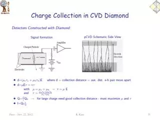
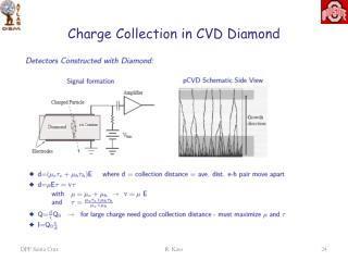
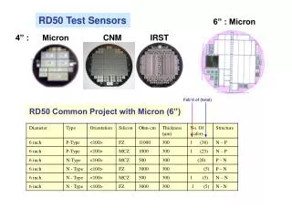
Charge Multiplication Detectors • 1 cm x 1 cm, n-in-p FZ strip detectors developed by MICRON • Detectors aim to enhance the electric field near the readout strips • Sensors of various strip width and pitch were produced, as well as sensors with floating and biased intermediate strips between readout strips • 5 type of wafers were produced: standard, double diff. time, double implant energy, thick and thin • IV, CV, C interstrip, and CCE measurements have been carried out [L. Atlan, 20th RD50 workshop, 2012] CERN RD50 Workshop, Geneva
1/C2 [1/nF2] Vbias [Volts] CERN RD50 Workshop, Geneva
ALIBAVA Readout System • Charge collection measurements are done through the ALIBAVA readout system • The daughterboard carries 2 analog front-end ASIC (Beetle) chips, which perform amplification and shaping of the signal • The analog signal is sent to the motherboard, controlled by an FPGA, and converted into digital counts using a 10-bit ADC (Analogue to Digital Converter) • The raw data is sent to a PC from the motherboard using a USB connection, and analyzed by custom software based off the ROOT framework CERN RD50 Workshop, Geneva
Beta Source Measurements • MIPs from a 90Sr source are used to perform charge collection measurements • Time between trigger signal and edge of a 10 MHz clock is measured by the ALIBAVA TDC • For each event, channel with largest SNR is chosen, and mean is calculated for each 1 ns time bin • Only events in 10 ns window around max are considered • Resulting spectrum is fitted with a convolution of a Gaussian and Landau distribution to determine MPV CERN RD50 Workshop, Geneva
Unirradiated Results • Full depletion reached at 100-125V • No charge multiplication observed up to 1100V on any sensor • Large spread of collected charge for sensors from a given wafer, no clear correlation on geometry • Most sensors show no breakdown up to 1100V CERN RD50 Workshop, Geneva
2935-2-27, 200V, CCE (ke) = 29.14 ± 1.61 CERN RD50 Workshop, Geneva
2935-2-27, 200V, CCE (ke) = 29.14 ± 1.61 • Cluster distribution has too many 2-Hit clusters • Sharp peaks around 0 and 1 of the η distribution with a flat area in-between • Signal on neighbors not as expected (superposition of two separate distributions?) • Asymmetry present in η distribution CERN RD50 Workshop, Geneva
Irradiated Detectors CERN RD50 Workshop, Geneva
Irradiated Detectors [G. Casse, 9th RESMDD, Florence 10 Oct 2012] • One sensor (2E imp w/p=6/80) shows clear signs of CM past 600V with no significant increase in noise • Detectors with floating intermediate strips increase charge compared to no intermediate strip detectors • Detectors with biased intermediate strips decrease charge compared to no intermediate strip detectors CERN RD50 Workshop, Geneva
Irradiated Detectors • CM only seen at Vbias > 600V • Both Extr. Diff. and 2E imp. Show signs of CM with respect to standard wafer • Lower w/p ratio leads to more pronounced multiplication (as expected) CERN RD50 Workshop, Geneva
Summary • The RD50 collaboration is investigating charge multiplication sensors as a viable option for radiation hard detectors • This study focuses on MICRON strip detectors of various geometries • No CM observed at 1e15 neq/cm2 for both proton and neutron irradiated samples • At 5e15 neq/cm2 one sensor (w/p=6/80 2E imp) shows pronounced signs of CM without a corresponding increase in the noise • Detectors with floating intermediate strips tend to enhance charge collection while detectors with a biased intermediate strip tend to decrease charge collection • Sensors with Double Diff. and Double Imp. Energy show enhanced charge for Vbias>600V at 5e15 neq/cm2, with lower w/p leading to more charge CERN RD50 Workshop, Geneva
Acknowledgements We would like to thank the irradiation teams and Ljubljana and Karlsruhe Discussions with Gianluigi Casse from Liverpool The RD50 community as a whole CERN RD50 Workshop, Geneva
BACKUP SLIDES CERN RD50 Workshop, Geneva
3D_S2, 20V CERN RD50 Workshop, Geneva
3D_S2, 20V • Cluster distribution looks as expected • Small asymmetry evident in the η distribution (possibly from the way the ASIC reads charge out from left to right, issues with the ALIBAVA firmware, or some other unknown cause) CERN RD50 Workshop, Geneva
W53-BZ4A-P4, 200V, CCE (ke) = 24.19 ± 1.33 CERN RD50 Workshop, Geneva
W53-BZ4A-P4, 200V, CCE (ke) = 24.19 ± 1.33 • Cluster distribution dominated by 2-Hit and 3-Hit clusters • η distribution makes no sense! • Hidden distribution more evident on neighbor’s signals • This detector used to calibrate our daughter boards (part of the reason we see too high of a signal on some MICRON sensors?) CERN RD50 Workshop, Geneva