Download
1 / 27
1.19k likes | 3.14k Views
SoC Design Flow. SoC Design Cycle. Concept Design Specification Engineering Specification Development Plan. Phase 1 – Specification. Spec. Sign-Off. ASIC Design, Full-Custom Design, DFT, Functional Verif. Plan Regression Analysis Pre-layout STA, Functional Review.

E N D
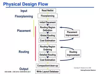
SoC Design Cycle • Concept • Design Specification • Engineering Specification • Development Plan Phase 1 – Specification Spec. Sign-Off • ASIC Design, Full-Custom Design, DFT, Functional Verif. Plan • Regression Analysis • Pre-layout STA, Functional Review Phase 2 – Functional Design Func. Sign-Off • Floorplan, Place & Route • Layout Verification • Post-layout STA • Post-layout review Phase 3 – Physical Design Post layout Sign-Off Tape-out Design
SoC Design Cycle • Prototype Acceptance Plan • Prototype Fabrication • Prototype Validation • Manufacturing Test Program • Prototype Acceptance Review Phase 4 – Prototype Fabrication & Validation Prototype Acceptance Sign-Off • EMI/EMC • Burn-in • Signal Integrity • Env compliance Phase 5 – Device Qualification Release To Production Sign-Off • Lessons Learnt • Future improvements • Possible Risks Phase 6 – Project Case Study End Cycle
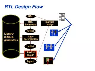
Different Levels of Abstraction Idea Conceptual idea about a functionality, that is thought through in the mind. A functional representation of the idea, in the form of a flow chart or other text information. (specification). Functional A model that can be verified by a concept simulation. This may be written using a HDL or other high level languages like C. Behavioral Register Transfer Level, which is the architectural HDL that can be converted into a logical representation. RTL RTL mapped into an equivalent gate level netlist using a target library. Logical Physical Physical specification that will help realize the device in silicon.
Specification • Engineering Specification • Functionality of SoC • Performance • External Interface • Pin Details • Modes of Operations • SW interface details • End application
Specification • Design Specification • Macro Architecture to validate • Interface • Throughput/Performance • Micro Architecture • Functional Partitioning • Block Architecture details • Block interface with timing diagrams • All the above to be in line with the engineering specification • Development plan with tasks, timeline and milestones (schedule)
Architecture Definition • Design Partition, macro and micro architecture It is a method used to divide the design into smaller functional elements, so that a very complex design is split into simpler inner level modules. What is the need for partitioning? • Divide and conquer idea. • Separate distinct functional blocks. • Focused verification efforts. • Reuse of a module across various designs and projects. • Workable size of a design for a set of tools. • Parallelizing work among team members. • Need to meet physical design challenges/constraints. Advantages: • Better results • Faster churning in tools (run time) • Easier top level integration
Design Phase - RTL • Translate Design Spec to RTL • Verilog/VHDL (use HDL) • Follow coding guidelines
Design Phase - Synthesis • Translate HDL into technology dependent gate level netlist • Perform Mapping • Perform Optimization • Timing • Area • Power • Insert DFT logic
Design Phase - Verification • Functional Verification • Test Bench design • Test scenarios • Test vectors (Deterministic, random) • Test coverage analysis • Line coverage • Expression coverage • Timing Verification • Design Performance • Design Rule checks • Signal integrity • Formal Verification • Equivalence checks
Why Verify • We need working parts • Time to market is very important • Cost of fixing problem (Pentium bug)
Physical Design – Layout • Floor planning • Pad Ring Design (IO, Vdd, Vss) • Placement (timing driven) • Clock Tree Design • Power Analysis • IR Drop (Dynamic & Static) • Routing (SI aware) • Noise Analysis • Design Rule Checks
Guidelines for routing analog signal wires Managing ESD and Latch-up across digital and analog IOs Decoupling Analog and digital power appropriately Providing adequate physical guard rings Suggesting process layer and design guidelines to handle Substrate Noise Providing the right IO selection Handling Mixed Signal Issues in Physical Design
Physical Design Verification • Checks for manufacturability of the design • Design Rule Checks (DRC) • Min spacing between wires • Thickness of wire • VIA size (other via checks) • Notch • LVS • Device inference • Shorts and Opens • Antenna Violations • Insert diode • Jog between layers
PDV - DRC • Design Rule Checks • Minimum spacing • Width • Minimum area
PDV - DRC • Design Rule Checks • VIA spacing • VIA area • Overlap
PDV - DRC • Design Rule Checks • Metal Density (Planarity)
PDV - LVS • Layout Vs Schematics • Device inference • Shorts and Opens During this task, the physical layout is checked against the functional gate-level schematic to ensure all intended connectivity has been maintained.
PDV - Antenna Antenna effects are long floating interconnects that act as temporary capacitors during the metalization process. Because a conducting path to ground does not exist at the time of metalization, a random discharge from the floating nodes can cause permanent gate oxidedamage Solutions: Antenna effects can be handled by inserting jumpers which minimizes the amount of charge collected by a floating node, by inserting buffers, or by inserting diodes near the input pins to provide a conduction path to ground
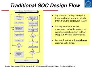
Explore Constraints Customer Constraints Design Req / Arch Converged Design DB Implement DB Implement RTL IP & LIB RTL Sample RTL/NL IP & LIB IP & Mem Req Analyze Identify design challenges Vendor/tech selection GDSII Package Info Test Info Converged Design DB Explore Constraints & Floorplan Implement Netlist Floorplan Physical DB Design Sign-Off Design ~Converged (5%) High-level Methodology Converge Tape-Out Implement Explore
Comprehensive Mfg Flow • Multiple Checklists • MS Project Schedule Tracking • Rigorous Document Control System Tapeout to RTP Flow Pre Tapeout First Silicon Validation Qualification RTP • 1st Silicon received • Debugging test program • Ship prototypes based on limited number of tests • Develop sort program • Finalize production test program • Ship fully tested parts • Issue validation report • Create BOM and test traveler • Review final qualification requirements • FIB or e-beam if needed • Identify golden units • Finalize characterization program • Complete ESD and Latch up • Start HTOL qualification procedure • Start pkg pre condition • Start temp. cycle • Start HAST qualification • Issue characterization report • Optimize test program • Issue Qual report • Develop test , assembly plan based on customer forecast • Complete plan for overseas test transfer if needed • Put all docs and procedure in document control system • Hold RTP review meeting • Develop yield monitor and enhancement program • Establish delivery performance metrics • Start 1st Eng and split lot per customer requirements • Manage wafer at different holding stages • Provide daily WIP report • Validate load board • Order Probe card and dummy probe wafer • Complete test program • Finalize assembly and marking documents • Review PCM data • Validate test vector through playback simulation • Test plan signoff • Review spec , Data sheet , Test Req. with customer Eng. team • Review Lot start, Characterization, Packaging, Qual with customer OPS team • Create detailed MS project file to track tasks and schedule • Start Burn-in , HAST boards design • Start Package design and procure substrate • Start Load board and Test program Dev. • Tapeout , Job view and Mask making TapeoutHandoff Docs Validation Check List Validation Report RTPCheck List SignoffRTP Docs
Case Study - Feedback • Lessons learnt • Good and Bad • Ways to improve the future designs • Yield • Schedule • Design Quality (reliability) • Cost • Predictability • Document the findings
Until next time… • Refresh on digital design • Identify a forum for discussion – with one point of contact • Refer the paper on Sequential Design • My contact • rpasirajan@hotmail.com