Download
1 / 1
10 likes | 114 Views
Constructing a New High Vacuum Semiconductor Synthesis Reactor for the Growth of ZnSnN 2 J. Sklenar , K. Kash Department of Physics, Case Western Reserve University, Cleveland, OH 44106.

E N D
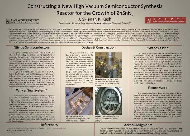
Constructing a New High Vacuum Semiconductor Synthesis Reactor for the Growth of ZnSnN2 J. Sklenar, K. Kash Department of Physics, Case Western Reserve University, Cleveland, OH 44106 The synthesis and study of group II-IV nitride semiconductors is an area of condensed matter physics that has not been rigorously explored. However, these materials are predicted and have been shown to be similar to the popular group III nitride semiconductors. Effective growth techniques of group III nitride semiconductors warrant a great amount of attention due to their usefulness in electronic devices such as LEDs. We believe group II-IV nitrides can be used in these same applications while possibly overcoming current limitations of group III nitrides. We have been interested in the synthesis of ZnSnN2 the group II-IV nitride semiconductor analog to InN, a group III material. This material has not yet been formed in any laboratory thus far, but it is crucial for it to be made and characterized in order for the group II-IV nitrides to fully realize their potential. Because this material has not yet been made, the phase space where it can be favorably created is not well defined. We have been constructing a system that can probe much of the remaining phase space where we believe this material can be stable based on earlier growth experiments and similarities with InN. This new system operates under high vacuum and utilizes a nitrogen plasma from an RF plasma generator. We will expose a Sn-Zn liquid melt within a heated crucible to the nitrogen plasma with the intent of precipitating ZnSnN2 crystals from the melt. We will use scanning electron microscopy and x-ray powder diffraction techniques to characterize the sample. Nitride Semiconductors The group III nitride semiconductor system of AlN-GaN-InN has been widely researched due to applications in optoelectronics, non-linear optical materials and solar cells. Currently there are limitations to this system in applications like LEDs. In this case GaN and InN are alloyed together in different percentages to create a tunable bandgap that encompasses the entire range of visible wavelengths. However, this GaN-InN subsystem faces quantum efficiency problems over a large portion of this spectrum. The group II-IV nitride semiconductor family of ZnSiN2-ZnGeN2-ZnSnN2 is predicted, and has been shown to have very similar properties to the group III materials. Furthermore, this group may have its own specific properties allowing it to be superior to the group III materials. In the case of the LEDs ZnGeN2 and ZnSnN2 are predicted to be better lattice matched possibly allowing this system to overcome the quantum efficiency problems faced by the group III system. Design & Construction Synthesis Plan The current plan is to synthesize the material from a melted composition of tin and zinc. The actual composition of the metals will be very tin rich (<80%) for a few reasons. Firstly, zinc is a very volatile metal that will tend to evaporate even at modestly high temperatures. It has been shown though that a tin rich alloy can suppress the vapor pressure of zinc. A tin rich system will also lower the melting temperature of the alloy well below even the lowest expected growing temperatures. Once the composition of the materials is chosen and inserted into the system the oxide impurities in the alloy will need to be removed before the two metals can fully be melted together. In order to do this hydrogen plasma can be flown through the system to remove the oxide layer as water vapor. After the oxide is removed a final growing temperature and pressure can be set and the experiment can be ran. A high vacuum system was built due to the use of plasma as the nitriding agent. The centerpiece of this system is a large six-way stainless steel cross. This cross can support all the necessary vacuum lines, electrical feedthroughs, measurement devices and even the plasma source. An experimental package was designed and built to hold and heat the crucible where the experiment will take place. It is designed to be inserted into the reactor cross as a non-permanent piece to give the system flexibility for future experiments. Figure 1. Picture of the six-way stainless steel reactor cross. The plasma source is mounted on the top face. Future Work Once growth experiments begin the first goal will be to establish whether or not ZnSnN2 is stable under the prescribed growing conditions. If a sample is obtained the first tests will be focused on verification of the material. This can be done first by visual identification using both an optical and scanning electron microscope, as II-IV semiconductors have hexagonal symmetry. The chemical composition and stoichimetric ratio of the elements within the sample can also be determined using EDX capabilities of the SEM. The last initial test of a sample will be x-ray powder diffraction to determine information about the ZnSnN2 crystal lattice. If initial experiments are able to determine ideal growing conditions for ZnSnN2 future experiments can focus on optimizing the quality of the grown sample. Why a New System? There were two main capabilities we needed in a growth system that motivated the construction of the new system. First we needed a system that could probe temperatures as low as 400 C. The temperature range chosen was based on the growing temperatures of InN the group III analog to ZnSnN2. This consideration made nitrogen plasma the most viable choice as a nitriding agent. The second capability needed is a straightforward growing mechanism. Because this project is interested in the phase space where this material is stable we are not as interested in obtaining large single crystals. Therefore, to grow the material we will expose a Sn-Zn melt within a heated crucible directly to the nitrogen plasma. Figure 2. Picture of the experimental package with heater and electrical connections. Figure 3. The interior of the cross with the installed experimental package. References Acknowledgments Report of the Basic Energy Sciences Workshop on Solid State Lighting, May22-24, 2006, http://www.e r.doe.gov/bes/reports/list.html . M. Drago, P. Vogt, W. Richter, Phys. Stat. Sol. 203, 2006. C. H. Su, T. Tung, A. Mubarak, and R. F. Brebrick. High Temperature Sciences 18:197, 1984. I would like to thank Professor Kash who made this project possible in the first place. Her expertise and advice has been invaluable. I would also like to thank Tim Peshek for helping start this project and for sharing his technical expertise without which this project would have not been possible.