Download
1 / 44
470 likes | 851 Views
Deuterium: Surface Science Meets CMOS Joseph W. Lyding Department of Electrical and Computer Engineering and Beckman Institute University of Illinois at Urbana-Champaign. Outline STM Nanofabrication on Si Deuterium Passivation Carbon Nanotubes on Silicon on III-V Semiconductors.

E N D
Deuterium: Surface Science Meets CMOSJoseph W. LydingDepartment of Electrical and Computer Engineering and Beckman InstituteUniversity of Illinois at Urbana-Champaign • Outline • STM Nanofabrication on Si • Deuterium Passivation • Carbon Nanotubes • on Silicon • on III-V Semiconductors
Benefits of UHV STM Atomic Resolution Analysis Detailed Spectroscopy Control Surface Chemistry Nanofabrication on Silicon Ultrahigh Vacuum (UHV) Scanning Tunneling Microscopy (STM) Thermal Drift ~ 0.1nm/h @ 300K
Piezoelectric Scanning Unit Tunneling Probe Sample Holder UHV STM Nanofabrication Surface Si(100)-2x1:H
Selective Chemistry Utilize strong chemical contrast between clean and H-Passivated Si. 440 K 3x1 650 K 2x1 Lyding et al., Appl. Phys. Lett. 64, 2010 (1994). UHV STM Hydrogen Resist Technique All UHV Technique Atomic Patterning Resolution Templates for Selective Chemistry Quantify Desorption Mechanisms
5 nm Hydrogen Desorption Regimes Shen, Lyding, Avouris et al., Science (1995) Direct ESD Regime: STM Electrons Excite Bonding-to-Antibonding Transition
3.5V 3V 2.5V Atomic Scale Resolution 2V Tunneling Regime Hydrogen Desorption Regimes Shen, Lyding, Avouris et al., Science (1995) Vibrational Heating Regime: Tunneling Electrons Excite Si-H Vibrations
C60 NBE Cu(Pc) NH3-Cu(Pc) Molecular Arrays on Silicon
Deuterium Passivation for Silicon Technology STM – CMOS Analogy Giant Isotope Effect Effect on Hot-Carrier Degradation Unraveling Degradation Mechanisms Processing Issues
Deuterium: CMOS/STM Analogy Joe Lyding and Karl Hess Key Collaborator: Isik Kizilyalli SiO2 SiO2 n- n- n+ n+ p-Si CMOS STM H H Lyding et al., Appl. Phys. Lett. 64, 2010 (1994).
Hydrogen ~100 Deuterium Large Isotope Effect in Direct Desorption Regime Giant Deuterium Isotope Effect Observed in STM Experiment Abeln, Avouris, Lyding 1995
3V H 11 K Hydrogen ~1014 D 11 K ~100 Deuterium Foley, Avouris, Lyding PRL 1998 Large Isotope Effect in Direct Desorption Regime Enormous Isotope Effect in Vibrational Heating Regime Giant Deuterium Isotope Effect Observed in STM Experiments Abeln, Avouris, Lyding 1995
Deuterium Passivation for Silicon Technology STM – CMOS Analogy Giant Isotope Effect Effect on Hot-Carrier Degradation Unraveling Degradation Mechanisms Processing Issues
Hydrogen Hydrogen Deuterium Deuterium Initial CMOS Deuterium Experiment 10X-50X Lifetime Improvement using Deuterium J.W. Lyding, K. Hess, and I.C. Kizilyalli, Appl. Phys. Lett. 68, 2526 (1996).
Problem:Copper interconnect technology requires barrier nitride layer which also acts as a deuterium diffusion barrier. Solution:Use ND3 to fabricate deuterated barrier nitride, thereby creating a built-in source of deuterium.(32X improvement) Deuterium Incorporation - IBM Results Ference et al., IEEE Trans. Elec. Dev., April 1999
ONO triple dielectric G S D Poly-Si H N+ N+ D p+ p+ p-substrate Effects of Two-Step High Temperature Deuterium Anneals on SONOS Nonvolatile Memory Devices J. Bu, and M. H. White, IEEE Elec. Dev. Lett. 22, 17 (2001). After stressing for 107 cycles (-9V 1ms, +10V 1ms erase/write) H-Annealeddevice has2-yearretention time with 0.5V memory window D-Annealeddevice has10-yearretention time with 0.5V memory window
Deuterium Passivation for Silicon Technology STM – CMOS Analogy Giant Isotope Effect Effect on Hot-Carrier Degradation Unraveling Degradation Mechanisms Processing Issues
Gate h+ e- Oxide h+ P+ Silicon n-Si well Electron Trapping & Interface Trap Creation Interface Trap Creation Hole Trapping & Interface Trap Creation Hot-Carrier Degradation Mechanisms in p-Channel MOSFET’s K. Cheng, J. Lee, J. W. Lyding, Y. Kim, H. Lee, and K. Suh, IEEE Electron Device Lett. 22(2001) 188 Device Degradation is due to: (1) interface trap creation (large isotope effect) (2) oxide charge trapping (small isotope effect). Q:Can these two effects be separated?
Interface Trap Creation Electron Trapping Oxide charge trapping dominates p-channel device degradation when Vg<<Vd or VgVd, while interface trap creation is the dominant mechanism for a moderate Vg. Interface Trap Creation & Hole Trapping Dominant Degradation Mechanism in p-Channel MOSFET’s K. Cheng, J. Lee, J. W. Lyding, Y. Kim, H. Lee, and K. Suh, IEEE Electron Device Lett. 22(2001) 188. Low Vg stress Moderate Vg stress High Vg stress
Interface trap creation is the dominant mechanism for hot-carrier-induced degradation in n-channel MOSFET’s. Dominant Degradation Mechanism in n-Channel MOSFET’s K. Cheng, J. Lee, K. Hess, and J. W. Lyding, Appl. Phys. Lett. 78 (2001) 1882 Low Vg stress Moderate Vg stress High Vg stress
Evidence for Vibrational H/D Desorption at SiO2/Si Interface in Deep Sub-Micron Devices L = 0.18m Vds = 2.5V L = 0.35m Vds = 3.75V Vgs Vgs Desorption rate decreases (Direct ESD) Desorption rate increases (Vibrational ESD) Carrier energy decreases Current density increases Electric field decreases Vgs increases
Key Issue: Deuterium Incorporation Background Hydrogen Diffusion Barriers Deuterium Passivation for Silicon Technology STM – CMOS Analogy Giant Isotope Effect Effect on Hot-Carrier Degradation Unraveling Degradation Mechanisms Processing Issues
Conclusion:Deuterium incorporation is much more efficient when pre-existing hydrogen is eliminated. Degradation Mechanism of Gate Oxide under Uniform Stress * D. J. DiMaria et al., JAP, 78 (1995) 3883. # J. D. Bude, et al., IEDM,44 (1998) 179. # Z. Chen et al., EDL, 21 (2000) 24. # J. Wu et al., IRPS, 38 (2000) 310. # D. Esseni et al., IEDM, 46 (2000) 33.
Previously bonded hydrogen at the interface is not entirelyreplaced by deuterium with a one-step deuterium annealing process. Q:Can we devise a simple technique to determine the deuterium passivation fraction at the interface? Hot-Carrier Stress/Deuterium Annealing Cycles
BASIS Hydrogen and deuterium have different desorption rates during hot-carrier stress. (RH – R) = CD (RH – RD) CD–Deuterium passivation fraction RH, RD, R -interface trap generation rates of fully hydrogenated, fully deuterated and partially deuterated devices. CD is the slope of the plot of (RH – R) vs. (RH – RD). Advantage Electrical measurement that avoids complex physical analysis like TOF-SIMS, for example. Deuterium Passivation Fraction K. Cheng, J. Lee, K. Hess, and J. W. Lyding, IEEE Electron Device Lett. May (2001)
CD = 1-exp[-(kt)n] k = k0exp(-E/RT) Deuterium Incorporation Process
k = k0exp(-E/RT) The pre-existing hydrogen is replaced by a process involving the dissociation of molecular deuterium at the interface. Deuterium Incorporation Process Si • + H(D)Si-H(D) ~01 Si • + H2(D2)Si-H(D) + H(D) 1.51eV2 Si -H + DSi-D + H <0.2eV3 Si-H + D2 Si-D + HD 1.84eV4 1K. L. Brower et al. APL, 57 (1990) 162 2A. Stesmans APL, 68 (1996) 2723 3B. Tuttle et al. PRB, 59 (1999) 5493 4This work.
Drain Current Degradation Processing temperature is lowered by pre-stressing without compromising reliability improvement by deuterium. State-of-the-art CMOS technology requires a reduced thermal budget for the use of low-k dielectric materials. Lowering Processing Temperature by Pre-stress Step K. Cheng, J. Lee, and J. W. Lyding, Appl. Phys. Lett. 77 (2000) 2358-2360
Samsung Alpha Microprocessor Chips High Pressure Deuterium Processing Jinju Lee and Kangguo Cheng Deuterium Incorporation – High Pressure Processing Deuterium Pressure Furnace: 30 atm, 450 C Capability with 8” wafer
Deuteration Benefits of high pressure Reduced processing time Improved deuterium incorporation Detriment of high pressure Annealing-induced interface trap creation High Pressure Deuterium Process J. Lee, K. Cheng, Z. Chen, K. Hess, J. W. Lyding, Y. Kim, H. Lee, and K. Suh, IEEE Electron Device Lett. 21(2001) 221 Hydrogenation
Samsung CMOS (0.1 m, 1.2 V, Metal 4) H2:N2 (1 atm) 300°C (1 atm, 1 hr) 300°C (5 atm, 3 hr) 350°C (1 atm, 3 hr) Annealing Condition 350°C (5 atm, 3 hr) 350°C (10 atm, 3 hr) 400°C (5 atm, 3 hr) 400°C (10 atm, 3 hr) 450°C (1 atm, 3 hr) 0 100 200 300 400 Magnitude of Improvement Impact of Deuterium on Low V Technology Over 300X lifetime improvement observed for 0.1 mm, 1.2 V CMOS technology.
Deuterium Conclusions Large isotope effect observed in STM experiments translates to CMOS hot carrier degradation. Direct Desorption & Vibrational Heating Background hydrogen is the key processing issue. High Pressure Processing Channel hot carriers dominate degradation under wide range of bias conditions. Channel current density is a key factor.
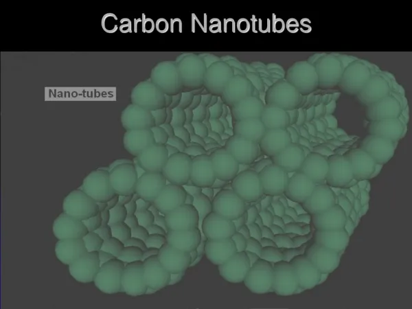
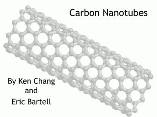
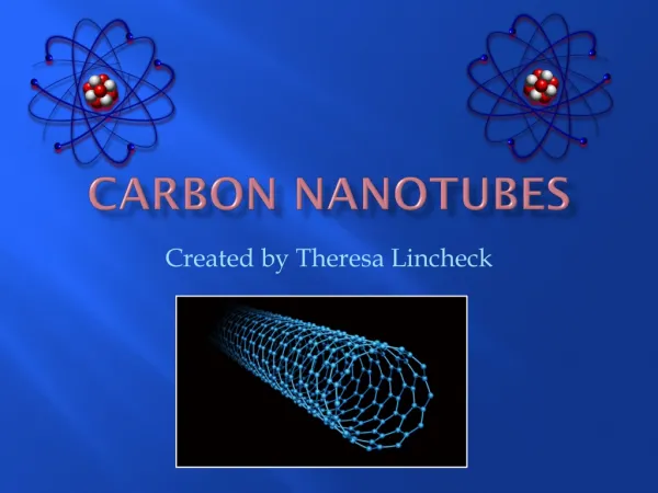
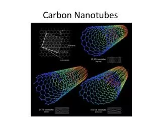
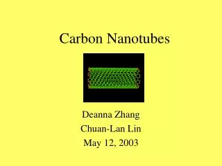
HiPco SWNTs deposited in dichlorobenzene onto Si(100)-21:H Rolling up a (10,10) nanotube z (n,n) armchair metallic CNT carbon nanotube Ch By Shigeo Maruyama, University of Tokyo, Japan Carbon Nanotubes Ambient-based solution deposition of SWNTs results in high levels of contamination and the requirement of an inert surface.
Dry Contact Transfer (DCT) Technique UHV STM Sample Holder Si(100)-2x1:H surface Fiberglass Applicator with SWNTs
SWNT height = 9.8 0.3 Å chiral sp2 carbon lattice 10 10 nm2 SWNT end cap DCT of SWNT onto Si(100)-2x1:H Peter Albrecht H-passivated Si(100)-21 DCT of SWNT onto GaAs(110) Laura Ruppalt DCT of SWNTs onto H-Si(100) and GaAs(110)
STM Topograph 10 nm DCT method results in ultra-clean depositon of isolated SWNTs rather than bundles. The DCT method can be generalized for the deposition of nearly any nanostructure onto nearly any surface. Nanotube Alignment Following DCT 1.1 nm 2mm x 2mm AFM image of sample following STM experiment
STM Topograph Parallel 7 Parallel 6 5 4 3 differential conductance dI/dV (a.u.) 2 1 Perpendicular 2 nm Perpendicular 10 nm Nanotube – Substrate Interactions: Clean Si(100) Orellana, et at., Phys. Rev. Lett. 91, (2003)
<110> Nanotube – Substrate Interactions: GaAs(110) 19.5 nm x 19.5 nm, empty states image I=15 pA, V=1.7 V Yong-Hyun Kim, M. J. Heben, and B.S. Zhang, Phys. Rev. Lett. 92, 176102 (2004)
NT B (not aligned) NT A (not aligned) NT B (not aligned) 39.1 nm, 40 pA –1.4V 1.6 Conduction Band NT A (aligned) 1.2 Ec=0.087 0.8 Ec=0.344 Eg=0.91 0.4 Eg=0.90 Applied Bias (V) 0 Eg=0.94 Eg=0.77 -0.4 Ev=0.047 Ev=0.200 -0.8 Valence Band NT A (not aligned) NT B (not aligned) NT A (aligned) NT B (not aligned) -1.2 -1.6 Nanotube on InAs: Substrate Alignment Effect Alignment shifts the bandgaptomore n-type character(compared to the misaligned case) Alignmentshrinks the band gap(compared to the misaligned case)
2222 nm2 STM topograph -1.5 V, 20 pA After ESD of hydrogen +7 V, 0.1 nA, 10-4 C/cm Patterned clean Si orthogonal to SWNT 3030 nm2 STM topograph -1.5 V, 20 pA Carbon Nanotube & STM Lithography
Summary Statement Atomistic View Provides new insight into old problems: Hot Carrier Degradation Provides useful information about new problems: Nanotube-Semiconductor Interfaces
Acknowledgements Students Peter Albrecht Laura Ruppalt Noureddine Tayebi Former Students Kangguo Cheng Eddie Foley Mark Hersam Postdoc Jinju Lee Industry Dr. Isik Kizilyalli – Lucent/Agere Dr. Phaedon Avouris - IBM Funding Office of Naval Research
Thank you, Karl Best wishes to you and Sylvia