
Understanding Defect-Related Recombination and Free Carrier Diffusion in GaAs Semiconductors
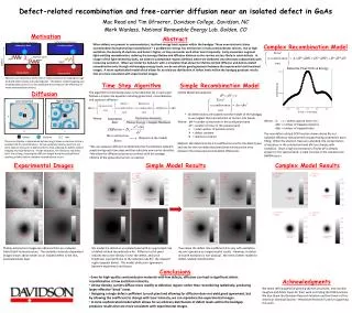
This study investigates the effects of defects in GaAs semiconductors, focusing on how localized energy levels within the bandgap lead to heat-generating recombination, which is detrimental to device efficiency. At high excitation, interactions between electrons and holes increase, prompting light-emitting recombination and reducing the likelihood of carriers reaching defects. Experimental photoluminescence images reveal isolated dark regions corresponding to defects, where a sophisticated model improves agreement between experimental and simulated results. Findings underscore the critical impact of diffusion and recombination processes on semiconductor performance.

Understanding Defect-Related Recombination and Free Carrier Diffusion in GaAs Semiconductors
E N D
Presentation Transcript
Defect-related recombination and free-carrier diffusion near an isolated defect in GaAs Mac Read and Tim Gfroerer, Davidson College, Davidson, NC Mark Wanlass, National Renewable Energy Lab, Golden, CO Motivation Abstract When defects are present in semiconductors, localized energy levels appear within the bandgap. These new electronic states accommodate heat-generating recombination – a problematic energy loss mechanism in many semiconductor devices. But at high excitation, the density of electrons and holes is higher, so they encounter each other more frequently. Early encounters augment light-emitting recombination, reducing the average lifetime and diffusion distance so the carriers are less likely to reach defects. In images of the light emitted by GaAs, we observe isolated dark regions (defects) where the darkened area decreases substantially with increasing excitation. When we model the behavior with a simulation that allows for lifetime-limited diffusion and defect-related recombination only through mid-bandgap energy levels, we do not obtain good agreement between the experimental and simulated images. A more sophisticated model which allows for an arbitrary distribution of defect levels within the bandgap produces results that are more consistent with experimental images. Complex Recombination Model Radiative Recombination Defect-related Recombination Conduction Band Conduction Band - - Defect Level ENERGY HEAT HEAT LIGHT 100 µm 100 µm + + Electrons can recombine with holes in semiconductors by hopping through localized defect states and releasing heat. This defect-related trapping and recombination process is a loss mechanism that reduces the efficiency of many semiconductor devices. Time Step Algorithm Simple Recombination Model Valence Band Valence Band Diffusion The algorithm to find steady state carrier densities (n) in each pixel follows a simple rate equation including generation, recombination, and Laplacian diffusion: Simple Model Assumptions: * All defect states are located near the middle of the bandgap so we neglect thermal excitation of carriers into bands. Method: We determine the 2 A coefficients (one for the defect pixel and one for the non-defective pixels) that minimizes the error between the measured and simulated efficiencies. 100 µm 100 µm Where: dN = number of electrons in the conduction band dP = number of holes in the valence band n = total number of excited carriers A = defect constant B = radiative constant Where: Where: Aτ = 1 / defect capture time (1/τ ) dDn = number of trapped electrons dDp = number of trapped holes Low-excitation High-excitation + - + d The new defect-related DOS function shown above fits our radiative efficiency measurements by generating asymmetric band filling. When the electron traps are saturated, the concentration of electrons in the conduction band dN rises sharply with excitation. Since a high concentration of holes dP is already present in the valence band, a rapid increase in the radiative rate BdPdN occurs. - - (Depend on the model) D D y y The carrier lifetime is determined by how long it takes an electron to find a suitable hole for recombination. At low excitation density, electrons are more likely to encounter a defect before a hole, allowing for defect-related trapping and recombination. At high excitation, the electrons and holes don’t live as long, reducing the diffusion length d and the probability of reaching a defect before radiative recombination occurs. 100 µm 100 µm + + + • We use Laplacian diffusion to determine the flux between adjacent pixels during each time step and then calculate new carrier densities. • We allow the diffusion process to continue until the average lifetime of the generated carriers is reached. - - d x x Defect Electron Hole D - + Experimental Images Simple Model Results Complex Model Results 100 µm 100 µm Photoluminescence images are obtained from an undoped GaAs/GaInP heterostructure. The excitation intensity-dependent images shown above center on an isolated defect in the thin, passivated GaAs layer. We model the defect as an isolated pixel with an augmented rate of defect-related recombination An. Diffusion to this pixel reduces the carrier density n near the defect, and since brightness is proportional to the radiative rate Bn2, the adjacent region appears darker. This model yields poor agreement between experiment and theory. If we allow the defect rate coefficient A to vary with excitation, we can reproduce our experimental results. However, variation of A with excitation is non-physical. We need a better model for defect-related recombination. Conclusions • Even for high-quality semiconductor materials with few defects, diffusion can lead to significant defect recombination at low excitation intensity. • At low density, carriers diffuse more readily to defective regions rather than recombining radiatively, producing larger effective “dead” areas. • Assigning a single defect coefficient to each pixel and allowing for diffusion does not yield good agreement, but by allowing the coefficient to change with laser intensity, we can reproduce the experimental images. • A more sophisticated model which allows for an arbitrary distribution of defect levels within the bandgap produces results that are more consistent with experimental images. Acknowledgments We thank Jeff Carapella for growing the test structures, and Caroline Vaughan and Adam Topaz for their work on finding the DOS functions. We also thank the Davidson Research Initiative and the Donors of the American Chemical Society – Petroleum Research Fund for supporting this work.