Download
1 / 1
20 likes | 260 Views
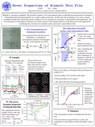
Grazing angle XRD. Novel Properties of Bismuth Thin Film 肖顺豪 导师:金晓峰 Department of Physics, Fudan University, Shanghai 200433.

E N D
Grazing angle XRD Novel Properties of Bismuth Thin Film 肖顺豪 导师:金晓峰 Department of Physics, Fudan University, Shanghai 200433 Bulk Bi is a prototype semimetal. The possible existence of its semiconductor phase in thin film has attracted lots of attentions both theoretically and experimentally, yet is still a controversial issue. In this work, the conductance of a series of single crystalline bismuth films epitaxially grown on BaF2(111) were measured as a function of film thickness and temperature, and the semimetal to semiconductor transition was clearly observed. The transport behavior in Bi film can be well explained by considering the coexistence of a metallic surface state and a semiconductor film. III. Indication of metallic surface and semiconductor film I. The Semiconductor-to-Semimetal transition It was predicted that with the decrease of thickness, a semimetal to semiconductor transition would happen because of the quantum size effect Similar behavior before 15~nm: very small conductance in thinner film; abrupt increasing in phase transition region. After completing the transition, the conductance became linear dependent on thickness at 300~K. At 5~K the conductance became thickness independent. I II V. N. Lutskii, JETP Lett. 2, 245 (1965), V.B. Sandomirsjii, JETP 25, 101 (1967) I II II. Samples Epitaxial Bismuth thin film on BaF2 (111) substrate constant The growth process involving two phases and three steps which is similar to the growing steps on Silicon(111) substrate There are two phases of bismuth in the growth process on BaF2(111): 1. Polycrystalline {012} pseudo-cubic phase 2. Hexagonal phase start to appear 3. The whole film turns into hexagonal phase Thickness dependent conductance at different temperature: distinctive behavior after 15nm T. Nagao,J.T. Sadowski, T. Sakurai PhysRevLett_93_105501(2004) IV. The novel transport properties of bismuth thin film The competition between metallic surface state and bulk semiconductor give rise a valley in the conductance – temperature curve. • V. Summary • The semiconductor phase of bismuth thin film does exist • The uncommon transport behavior is due to the competition of semiconductor bulk and metallic surface state