Download
1 / 24
250 likes | 424 Views
Development and Characterization of STT-RAM Cells. Team Members: Kang L Wang (PI) - UCLA Pedram Khalili (PM) – UCLA Ken Yang (Investigator) - UCLA Dejan Markovic (Investigator) - UCLA Hongwen Jiang (Investigator) - UCLA Yaroslav Tserkovnyak (Investigator) - UCLA

E N D
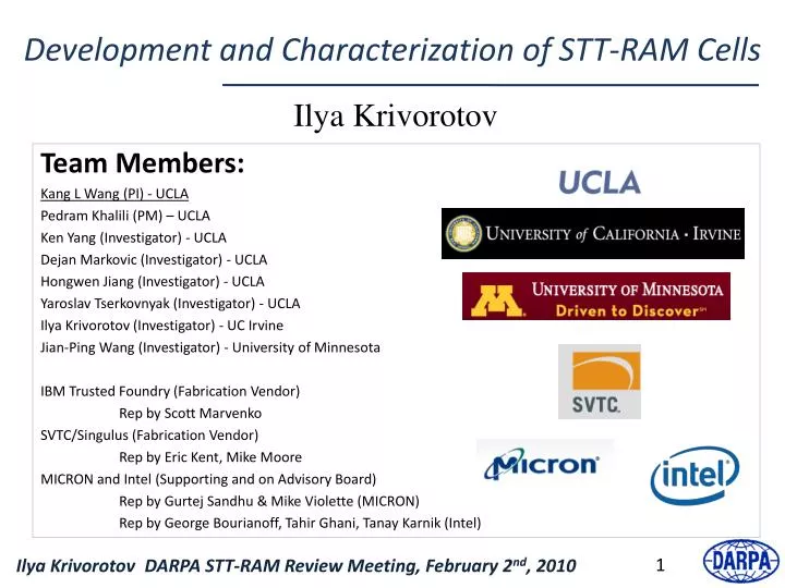
Development and Characterization of STT-RAM Cells Team Members: Kang L Wang (PI) - UCLA Pedram Khalili (PM) – UCLA Ken Yang (Investigator) - UCLA Dejan Markovic (Investigator) - UCLA Hongwen Jiang (Investigator) - UCLA Yaroslav Tserkovnyak (Investigator) - UCLA Ilya Krivorotov (Investigator) - UC Irvine Jian-Ping Wang (Investigator) - University of Minnesota IBM Trusted Foundry (Fabrication Vendor) Rep by Scott Marvenko SVTC/Singulus (Fabrication Vendor) Rep by Eric Kent, Mike Moore MICRON and Intel (Supporting and on Advisory Board) Rep by Gurtej Sandhu & Mike Violette (MICRON) Rep by George Bourianoff, Tahir Ghani, Tanay Karnik (Intel) Ilya Krivorotov
Outline • STT-RAM optimization to approaching Phase 1 metrics • Free layer dimensions (area, aspect ratio, thickness) • Optimal MgO thickness • Optimal write voltage pulse amplitude and duration • Energy-efficient switching with non-collinear polarizer • Measurement techniques • Thermal stability • Switching with short voltage pulses • Recent results and metrics update • Summary and Outlook
Where we were 3 month ago • At the pervious review meeting we were reported initial results of non-optimized STT-RAM cells. They showed the following metrics parameters: • Write energy per bit 7.5 pJ • Write time 2.5 ns • Upper bound on thermal stability: • < 90 • Lower bound on endurance of 105 • Since the review meeting in November 2009, we have substantially improved the metrics through STT-RAM device optimization Data reported in November 2009 Voltage at the sample, Vs
STT-RAM Optimization: Free Layer Dimensions - critical current for STT-RAM Fundamental constants and material parameters l w • For a given material, to reduce Icone should decrease the free layer volume V without sacrificing thermal stability d - Thermal stability • To decrease volume V while keeping constant, we must increase thickness and decrease width w
STT-RAM Optimization: Barrier Thickness • - Since energy per write is I2R tw, low RA MgO also decreases energy per write • Low TMR is signature of pinholes an lower-voltage dielectric breakdown • MgO thickness with lowest RA that still has high TMR is needed RA VS MgO thickness TMR ratio VS MgO thickness We found that the optimal MgO thickness for I-STT-RAM devices is right at the knee in RA and TRM plots versus MgO thickness.
STT-RAM Optimization: Write Pulse Shaping For short switching times, switching time versus pulse duration is well fit by the following functional dependence: V0 is the (zero-temperature) critical voltage for switching This is a signature of quasi-ballistic switching dominated by angular momentum transfer rather than temperature This (V) allows us to determine the optimal write voltage V for minimizing the energy per write
STT-RAM Optimization: Write Pulse Shaping Energy per write: Write time: - E(V) has a minimum at V=2V0 - Minimum energy per write is at twice the critical voltage - This is consistent with our data
STT-RAM Optimization: Write Pulse Shaping Experimental data Theory 0.46 pJ Predicted write energy minimum is experimentally observed
STT-RAM Optimization: Non-collinear structures • Micromagnetic simulations show that for collinear free and fixed layer geometries: • there is long incubation time between the leading edge of the write pulse and the nanomagnet switching • energy is wasted on excitation of non-uniform modes FL Barrier PL AFM
STT-RAM Optimization: Non-collinear structures The incubation time results from small initial spin torque in the collinear geometry (spin torque ) Polarizer that is non-collinear with the free layer provides larger spin torque, accelerates the switching process Collinear free and fixed layers, simulations Non-collinear free and fixed layers, simulations
Materials for non-collinear structures perpendicular filed We developed materials with perpendicular anisotropy for STT-RAM structures with non-collinear magnetizations
STT-RAM Optimization: Non-collinear structures • - Our measurements of switching of devices with non-collinear magnetization revealed deep sub-ns switching. • - This is a salient feature of precessional switching due to perpendicular polarizer • Pulse shaping is expected to further improve the energy per write Device shape and magnetic multilayer optimization is also expected to significantly improve the non-collinear device performance compared to this initial demonstration. This device concept is very promising for meeting Phase 2 metrics.
Measurement Techniques of Metrics • Energy per write and write time • Switching in response to ns and sub-ns pulses • Thermal stability measurements • Thermally activated switching • Field-assisted switching • Hard axis hysteresis loop measurement
Switching by Short Voltage Pulse Pulse Generator (0.1 – 10 ns pulse width) STT-RAM element Multimeter (resistance measurement) DMM • Pulses of variable duration are sent to the sample • Sample resistance before and after the switching is measured • - Probability of switching is determined
Voltage of Short Pulse at the Sample • Voltage at the sample is a sum of incident and reflected voltages • Since the sample resistance is much higher than 50 , the voltage at the sample is nearly doubled compared to the incident voltage • We use a pulse generator that absorbs the reflected pulse without affecting the incident pulse Vin Vs Vref Rs
Thermal Stability: Method 1 Thermally-Activated Switching • - Switching in response to long, relatively low-voltage pulses • Switching time histograms are measured and switching voltage versus pulse duration is obtained • Extrapolation of the plot of switching voltage versus pulse duration down to zero voltage, (V=0) gives the bit lifetime and thermal stability Fitting to exponential function gives the average bit life time, , at a given voltage
Method 1 Thermally-Activated Switching • Applying current-assisted switching, lower bound on thermal stability is determined. • This is only a lower bound due to current noise, ohmic heating and possible current-induced magnon excitation Single switching attempt sequence Ri Rf Ri Rf Ri Rf Quasi-ballistic switching Thermally Activated Δ=63; ts(0 Volt) = 31 billion years Train of 10,000 write/reset pulses 10,000,000 switching attempts Time [s]
Method 2: coercivity vs field sweep rate • Another approach to determining thermal stability is to measure the sweep rate dependence of the coercive field. The coercive field under the sweep time based on the Neel-Arrhenius model is: Resistance vs magnetic field at different sweep time. Coercivity vs sweep time.
Thermal Stability: Method 3 Hard-axis Loop Estimating the anisotropy field as: Hard Axis Hysteresis Loop free free • - Anisotropy field estimated by this method is ~ 570 Oe • Micromagnetic OOMMF simulations give the hard-axis saturation field ~ 520 Oe. • The origin of the hard-axis loop asymmetry is not clear • - Using 520 Oe value, the thermal stability estimate gives an upper bound on thermal stability HL HR
Current status of STT Cells As a result of a combination of aforementioned STT-RAM optimization procedures, device performance has been substantially improved since the last review meeting. Optimized device quasistatic characteristics:
Switching of Improved STT-RAM Cells In the optimized devices, at the optimal voltage pulse amplitude, write energy of 0.46 pJ has been achieved. >55 0.46 pJ
Two Thermal Stability Measurements of I-STT Thermally activated switching – lower limit for Hard axis saturation – upper limit for Δ=55 HK 650 Oe as average of HL and HR -> 90 Two measurements give the bounds on the thermal stability 55<<90 HK 550 Oe from micromagnetic simulations
Summary • We made a significant progress towards optimizing the performance of STT-RAM cell through device optimization: • Free layer dimensions (area, aspect ratio, thickness) • Optimal MgO thickness • Optimal write voltage pulse amplitude and duration • Energy-efficient switching with non-collinear polarizer • All Phase 1 metrics are clearly within reach with modest further optimization. • We are also on the way towards meeting Phase 2 metrics using non-collinear structures.