Download
1 / 1
10 likes | 80 Views
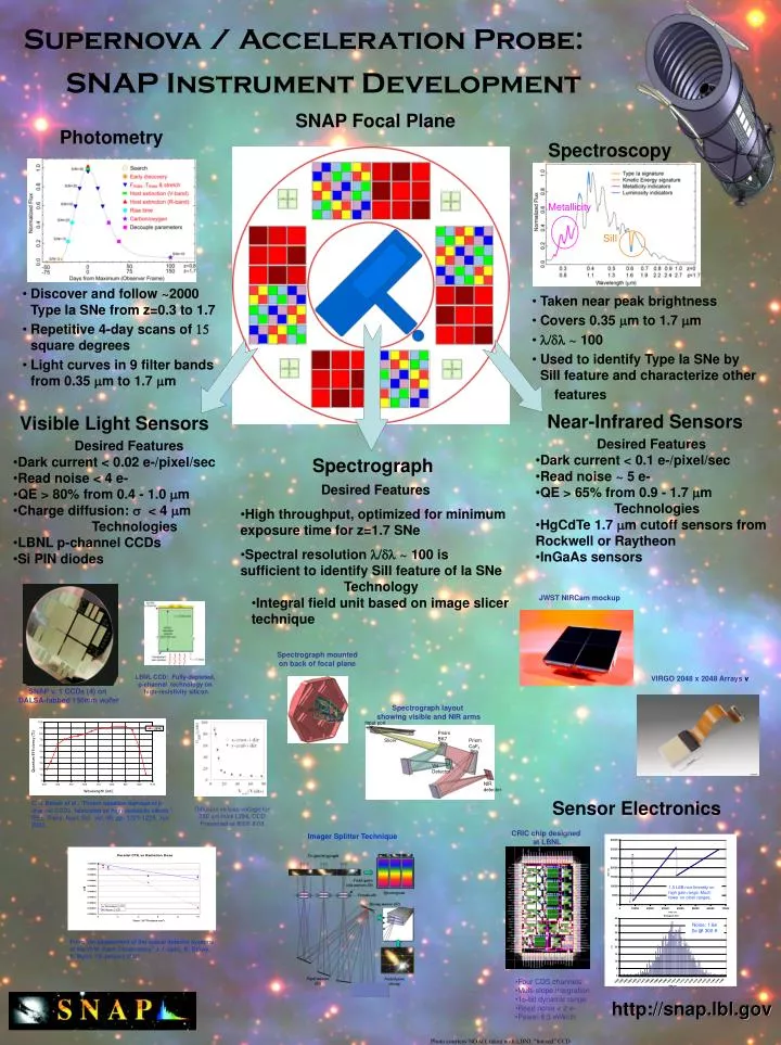
Input port. Prism BK7. Slicer. Prism CaF 2. Vis Detector. NIR detector. Supernova / Acceleration Probe:. SNAP Instrument Development. SNAP Focal Plane. Photometry. Spectroscopy. Metallicity. SiII. Discover and follow ~2000 Type Ia SNe from z=0.3 to 1.7

E N D
Input port Prism BK7 Slicer Prism CaF2 Vis Detector NIR detector Supernova / Acceleration Probe: SNAP Instrument Development SNAP Focal Plane Photometry Spectroscopy Metallicity SiII • Discover and follow ~2000 Type Ia SNe from z=0.3 to 1.7 • Repetitive 4-day scans of 15 square degrees • Light curves in 9 filter bands from 0.35 mm to 1.7 mm • Taken near peak brightness • Covers 0.35 mm to 1.7 mm • ~ 100 • Used to identify Type Ia SNe by SiII feature and characterize other features Near-Infrared Sensors Visible Light Sensors • Desired Features • Dark current < 0.1 e-/pixel/sec • Read noise ~ 5 e- • QE > 65% from 0.9 - 1.7 mm • Technologies • HgCdTe 1.7 mm cutoff sensors from Rockwell or Raytheon • InGaAs sensors • Desired Features • Dark current < 0.02 e-/pixel/sec • Read noise < 4 e- • QE > 80% from 0.4 - 1.0 mm • Charge diffusion: s < 4 mm • Technologies • LBNL p-channel CCDs • Si PIN diodes Spectrograph • Desired Features • High throughput, optimized for minimum exposure time for z=1.7 SNe • Spectral resolution ~ 100 is sufficient to identify SiII feature of Ia SNe • Technology • Integral field unit based on image slicer technique JWST NIRCam mockup Spectrograph mounted on back of focal plane LBNL CCD: Fully-depleted, p-channel technology on high-resistivity silicon VIRGO 2048 x 2048 Arrays v SNAP v. 1 CCDs (4) on DALSA-fabbed 150mm wafer Spectrograph layout showing visible and NIR arms Sensor Electronics C. J. Bebek et al., “Proton radiation damage in p-channel CCDs fabricated on high-resistivity silicon,” IEEE Trans. Nucl. Sci. vol. 49, pp. 1221-1225, Jun. 2002. Diffusion vs bias voltage for 250 mm thick LBNL CCD Presented at IEEE 8/03 CRIC chip designed at LBNL Imager Splitter Technique 1.5 LSB non-linearity on high gain range. Much lower on other ranges. Noise: 1.6e 2e @ 300 K From “An assessment of the optical detector systems of the W.M. Keck Observatory,” J. Beletic, R. Stover, K Taylor, 19 January 2001. • Four CDS channels • Multi-slope integration • 16-bit dynamic range • Read noise < 2 e- • Power 6.5 mW/ch http://snap.lbl.gov Photo courtesy NOAO, taken with LBNL “hot red” CCD