Download
1 / 25
250 likes | 317 Views
The uA741 Operational Amplifier. Outline. Brief History Stages DC Bias Point Analysis Small Signal Analysis Concluding Remarks. Brief History. 1964 – Bob Widlar designs the first op-amp: the 702. Using only 9 transistors, it attains a gain of over 1000 Highly expensive: $300 per op-amp

E N D
Outline • Brief History • Stages • DC Bias Point Analysis • Small Signal Analysis • Concluding Remarks
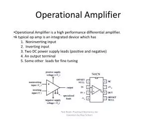
Brief History • 1964 – Bob Widlar designs the first op-amp: the 702. • Using only 9 transistors, it attains a gain of over 1000 • Highly expensive: $300 per op-amp • 1965 – Bob Widlar designs the 709 op-amp which more closely resembles the current uA741 • This op-amp achieves an open-loop gain of around 60,000. • The 709’s largest flaw was its lack of short circuit protection.
Brief History (cont) • After Widlar left Fairchild, Dave Fullagar continued op-amp design and came up with the uA741 which is the most popular operational amplifier of all time. • This design’s basic architecture is almost identical to Widlar’s 309 op-amp with one major difference: the inclusion of a fixed internal compensation capacitor. • This capacitor allows the uA741 to be used without any additional, external circuitry, unlike its predecessors. • The other main difference is the addition of extra transistors for short circuit protection. • This op-amp has a gain of around 250,000
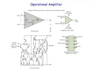
Stages • Input Differential Stage • Intermediate Signal-Ended High-Gain Stage • Output Buffering Stage • Current Source / Short Circuit Protection
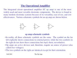
Input Differential Stage The input stage consists of the transistors Q1 through Q7 with biasing performed by Q8, Q9, and Q10. Transistors Q1 and Q2 are emitter followers which causes input resistance to be high and deliver the differential input signal to the common base amplifier formed by Q3 and Q4. Transistors Q5, Q6, and Q7, and resistors R1, R2, and R3 form the load circuit of the input stage. This portion of the circuit provides a high resistance load. Transistors Q3 and Q4 also serve as protection for Q1 and Q2. The emitter-base junction of Q1 and Q2 breaks down at around 7V but the pnp transistors have breakdown voltages around 50V. So, having them in series with Q1 and Q2 protects Q1 and Q2 from an accidental connection between the input terminals.
Intermediate Single-Ended High-Gain Stage The second stage is composed of Q16, Q17, Q13B, and the resistors R8 and R9. Transistor Q16 acts as an emitter follower giving the second stage a high input resis- tance. Transistor Q17 is a common-emitter amplifier with a 100-Ώ resistor in the emitter. The load of this amplifier is composed of the output resistance of Q13B. This use of a transistor as a load resistance is called active load. The output of this amplifier (the collector of Q17) has a feedback loop through Cc. This capacitor causes the op-amp to have a pole at about 4Hz.
Output Buffering Stage The Output Stage consists of the complimentary pair Q14 and Q20, and a class AB output stage composed of Q18 and Q19. Q15 and Q21 give short circuit protection (described later) and Q13A supplies current to the output stage. The purpose of the Output Stage is to provide the amplifier with a low output resistance. Another requirement of the Output Stage is the ability to dissipate large load currents without dissipating large quantities of power. This is done through the class AB Out- put Stage.
Current Source / Short Circuit Protection • Transistors Q11 and Q12 form one half of a current mirror that is used to supply current to the entire op-amp. • Transistor Q10 is used to supply a bias current to the Input Stage, Q13B supplies the Second Stage, and Q13A supplies the Output Stage. • Transistors Q15, Q21, Q24, Q22, and resistors R6, R7, and R11 make up the short circuit protection circuit. For a more detailed description see your text. (Microelectronic Circuits by Sedra / Smith 4th addition, pg 813)
DC Analysis Reference Bias Current • This current is generated by Q11, Q12 and resistor R5. From these, we can write: • From this value of IREF, the current in the collector of Q10 can be calculated. • This value (IC10) is twice the value of I (which is used later in the DC analysis.
DC Analysis (cont) Input Stage Using the value IC10 found before, the analysis unfolds as shown in the schematic. This analysis is done using the standard BJT, current mirror, and differential amplifier textbook equations.
DC Analysis (cont) Second Stage Assuming beta to be >> 0, the following DC biasing equations result
DC Analysis (cont) Output Stage Using the fact that Q13A delivers ¼ of IREF, the following outputs result: If Vbe is assumed to be 0.7V, the current in R10 is 18uA which causes the following: Since the base current of Q18 is IC18 / beta = 165u / 200:
DC Analysis (cont) Table of Results Below is a table that lists all of the transistors and their collector currents.
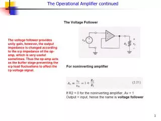
Small Signal Analysis To better visualize the various small signal properties of the uA741 op-amp, a simple inverting circuit is constructed around the op-amp. This circuit is the circuit that will be used in the following analysis. It has a gain of 100 (Rf / R).
Small Signal Analysis (cont) • Frequency Response The op-amp circuit is supplied by a 1mV AC signal and a Frequency analysis is performed. The inverting amplifier circuit outputs a gain of 100 until a frequency of 8kHz is reached. After this point, it attenuates at 20dB per decade until it reaches unity gain at 1MHz.
Small Signal Analysis (cont) • Transient analysis The op-amp circuit is now supplied with a 1mV 1kHz sinusoidal source and a transient analysis is performed. The op-amp outputs a 100mV signal that is the exact inverse of the input signal. This verifies that the op-amp is indeed magnifying the signal appropriately as well as inverting the signal.
Small Signal Analysis (cont) • Monte Carlo Analysis a. The resistors of the circuit are to be given a 2% tolerance and the frequency/transient analysis are to be performed again. b. Next, the beta values of the transistors are to be given a tolerance of 50%. c. Finally, the temperature of the circuit is varies from –150C to 100C
Monte Carlo Analysis The resistor values are allowed to vary by 2% • Transient Analysis The resistor values, as can be seen on the left, do cause changes in the output signal, however, the general output shape is retained. Note: The 61mV offset is still present
Monte Carlo Analysis The resistor values are allowed to vary by 2% • Frequency Response As is to be expected, the resistor variances have little (almost none) effect on the frequency response of the op-amp. This is expected because the resistors have no effect on the capacitances and poles of the amplifier.
Monte Carlo Analysis The transistor beta values are allowed to vary by plus/minus 50 • Transient Analysis As is evident by the plot on the left, the beta value of the transistors have very little effect on the output signal. The design of the uA741 op-amp is such that the circuit is beta independent. The plot on the right is a histogram showing the number of times that a particular output value (from the above simulation) occurred. As can be seen, a vast majority of the output signals are within 5mV of the expected value.
Monte Carlo Analysis The transistor beta values are allowed to vary by plus/minus 50 • Frequency Analysis As is evident by the simulation/histogram on the left, the uA741 operational amplifier’s frequency response is not effected by changes in beta. Once again, this is due to the op-amp’s relative beta independence. This beta independence is quite beneficial because in the mass production of transistors, their beta values can vary by a large amount. Having the op-amp operate regardless of beta variations assures that the amplifier will operate properly in a wide range of conditions.
Monte Carlo Analysis The temperature of the system is set to -150C, 0C, and 100C As can be seen by the simulation on the left, variances in temperature do not effect the shape of the output nor do they effect the amplitude of the output (the gain stays the same). Temperature does, however, effect the DC offset.
Concluding Remarks • The uA741 operational amplifier is a versatile circuit that is not adversely affected by outside interference. • Changes in beta, resistor values, and temperature have little effect on the op-amp. • This shows how well the uA741 was designed. • However, as technology continues to improve, CMOS amplifiers are beginning to become more popular than their BJT cousins.