Slide Note
0 likes | 18 Views
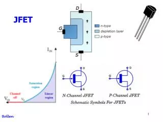
JFET, or Junction Field Effect Transistor, is a key component in electronic circuits used for switching and amplification. Unlike traditional transistors, JFET does not have PN-junctions but relies on a narrow channel of high resistivity material. It offers three terminals - Gate, Drain, and Source - and can be PNP or NPN based on doping type. The JFET operates in three regions - Active, Saturation, and Cut-off - providing flexible functionality in circuits like common source, common gate, and common drain configurations.

E N D
JFET PRESENTATION GT ECE INSTRUCTIONAL LABS SLIDES BY DANIEL TERRELL
WHAT IS A TRANSISTOR? • Three terminal active device made from semiconducting material • Acts as insulator or conductor by applying small signal voltage • Two Functions • Switching (Digital) • Amplification (Analog)
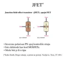
WHAT IS A JFET? • Junction Field Effect Transistor • JFET has no PN-junctions but instead has a narrow piece of high resistivity semiconductor material forming a “Channel” of either N-type or P-type • Creates Three Terminals • G – Gate, D – Drain, and S – Source • The JFET is a voltage controlled three terminal transistor that’s output is dependent on its type and the voltage applied to the gate of the transistor
TWO TYPES OF JFET • PNP vs. NPN • Dependent on doping type (P-type/N- type) • Direction of the conventional current flow between drain and source is dependent on the doping • PNP (N-type) – current goes from drain to source • NPN (P-type) – current goes from source to drain
THREE REGIONS • Active Region • Transistor operates as voltage controlled resistor • Saturation • Transistor operates as a good conductor • Cut-off • Transistor operates as an open source
THREE WAYS TO CONNECT JFET TO A CIRCUIT • Common Source Configuration • Voltage Gain used in frequency Amplifiers • Common Gate Configuration • Used in impedance matching circuits • Common Drain Configuration • Used to buffer amplifiers Common Source Configuration Common Gate Configuration Common Drain Configuration Common Source Common Gate Common Drain Characteristic Input Impedance High Low High Output Impedance High High Low Phase Shift 180o 0o 0o Voltage Gain Small loss High Low Current Gain High Low High Power Gain High Low Medium