Logic gate level
Logic gate level. Part 4: combinational devices. K-maps & don’t care conditions. It isn’t always necessary to process all possible input combinations, since some are never expected to be present

Logic gate level
E N D
Presentation Transcript
Logic gate level Part 4: combinational devices
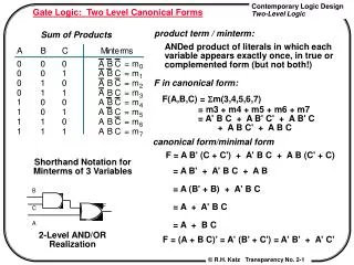
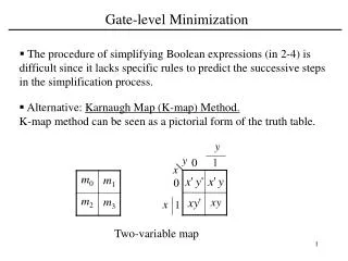
K-maps & don’t care conditions • It isn’t always necessary to process all possible input combinations, since some are never expected to be present • Such input combinations are called don’t care conditions, since we don’t care about the outputs they’d produce should they ever be present
K-maps & don’t care conditions • With don’t care condition present, you can arbitarily choose either 1 or 0 for output • Choice of output (1 or 0) for don’t care conditions can aid in minimization • Sigma notation for don’t care conditions: (x,y,z) + d(a,b) where x,y,z,a and b all represent lines in the function’s truth table • We represent don’t care conditions in a K-map with Xs
Example • K-map for X(a,b,c) = (2,4,6) + d(0,7) • With d.c. conditions, since we don’t care, we can choose to include, or not include, boxes with X designations in K-maps • X is “wildcard” condition – can be treated as either 1 or 0 • In K-map above, if minterm 0 is treated as 1 and 7 as 0, get • (0,2,4,6) = c’
Combinational Devices • Many devices have input line called an enable, which acts like on/off switch • if enable is 0, all outputs are 0 regardless of other inputs • if enable is 1, output depends on input to function that specifies device • AND gate can implement an enable
Selective inverter • Has data line & invert line • If invert = 1, output is complement of data • If invert = 0, output is data unchanged • Implement with XOR gate
Multiplexer • Device that selects one of several inputs to route to single output • Consists of set of data lines & control lines • control lines determine which data input will be output • n control lines can control 2n data lines
8-input multiplexer Combination of control line (s0-s2) inputs determines which of 8 data lines (d0-d7) is expressed as output value
Implementation of multiplexer • Each data line ANDed with combination of control lines • Result of ANDs is ORed together to get output • Illustration on next slide shows 4-input version of this scheme; 8-input version (like previous example) would involve 8 4-input AND gates
Binary decoder • Takes input from control lines and sets one of several output lines to 1, rest to 0 • Output value depends on input value(s)
Decoder with enable • When enable line is 1, device operates normally • When enable line is 0, all outputs are 0 • Requires extra input to each AND gate
Demultiplexer • Routes single input value to one of several output lines • Really just decoder with enable: input line connected to enable
Building the CPU • Control unit: portion of CPU that: • ensures synchronization of events – i.e. sending & receiving bits on the bus • selects next instruction • stores values in appropriate locations • Made up of combinational devices
Bus • Internal bus: common path connecting all registers in a register machine’s CPU • each register composed of multiple bits, all of which can be transferred simultaneously to another register • bus composed of parallel wires – as many lines as there are bits in registers • may also include control lines indicating which registers should send & receive • action must be coordinated, as bits from only one register at a time can be broadcast over bus • coordination requires timing mechanism
Putting it together • Parallel AND gates used to connect registers to bus • One input line to each gate is data waiting to be transmitted, second is select signal (CLOCK) • Date transmitted only if select signal is 1
Example: 2 8-bit registers tied to 8-bit bus with select (clock) signal
Strobing • When select signal is high, each gate allows signal to flow • clock (select) ANDed with each bit from registers • all bits transmitted simultaneously, and received simultaneously at destination register
Clock • Source of all select signals; generates pulses at fixed rate • Normal state is low (0); transmits 1 at regular interval • Speed measured in hertz: • 1 Hz = 1 cycle/second • 1 MHz = 1,000,000 cycles/second • 1 cycle ~ 1 step of fetch/execute cycle • Time interval between pulses measured in fractions of seconds – for PC, typically nanoseconds (1 s ~ 1/1,000,000,000 second)
Arithmetic Logic Unit • Part of the computer that computes • All operations performed using combinations of logic circuits • logical operations are performed by connecting operands bit-wise through ganged gates of appropriate type • arithmetic operations are also performed logically: operands connected bit-wise through ganged gates of appropriate type(s)
Performing arithmetic operations • Can break down any binary arithmetic operation into set of operations on pairs of bits • Each unique pair of bits combines to produce • result (0 or 1) • carry (0 or 1) when result is larger than either of the two operands • These 2 output bits can be viewed as single 2-bit number representing result of arithmetic operation on two 1-bit operands
Performing arithmetic operations • Example: addition of two operands produces the results shown in the truth table below: • Notes on truth table • First output (Sum) same as XOR • Second output (Carry) same as AND
Half adder • A half adder is the logical construction that implements the truth table on the previous slide • Half adders take single bits as input, produce 2 outputs
Full adder • Addition of two bits accomplishes only half the task of binary addition, unless we’re satisfied with working in single-digit numbers • To complete an addition operation, we must add the carry to the next (left) bit • Can construct full adder from half adders; carry from previous bit sum is ORed with carry from correct bit
Implementation of full adder from two half-adders By chaining together several of these constructs, we can build adders for multiple-digit numbers
Subtraction • Result column (difference) can be expressed as: ab + a’b’ • Carry column: a’b
Notes on adders • If last bit in series of half adders produces an non-zero carry, result will overflow • An adder constructed from a series of half adders is called a cascading adder – results cascade from right to left as previous carries must be determined before subsequent adds are performed
Adder as black box • Control unit delivers data to input registers in ALU • Device select signal triggers ALU to perform addition & send result to result register • Control unit causes result to be copied to its destination